Wafer-based optical pattern recognition targets using regions of gratings

a technology of optical pattern recognition and optical pattern, applied in the field of optical pattern recognition targets, can solve the problems of large pattern defects and incompatibility of structures

Inactive Publication Date: 2008-01-03
INTEL CORP
View PDF13 Cites 40 Cited by
  • Summary
  • Abstract
  • Description
  • Claims
  • Application Information

AI Technical Summary

Problems solved by technology

For some fabrication process technologies, the large patterns may have defect issues due to line-width and/or critical dimension (CD) control requirements

Method used


Image

  • Wafer-based optical pattern recognition targets using regions of gratings
  • Wafer-based optical pattern recognition targets using regions of gratings
  • Wafer-based optical pattern recognition targets using regions of gratings

Examples


Embodiment Construction

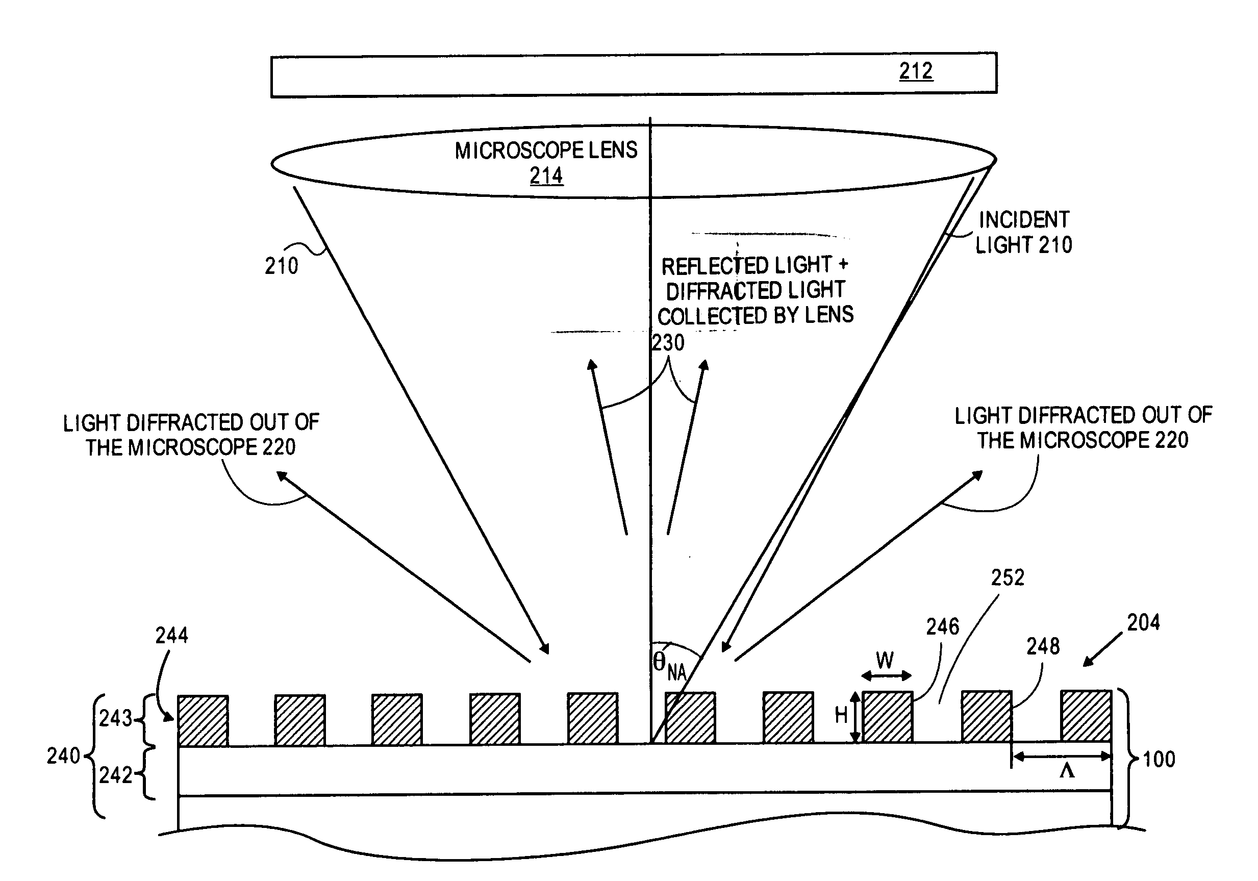
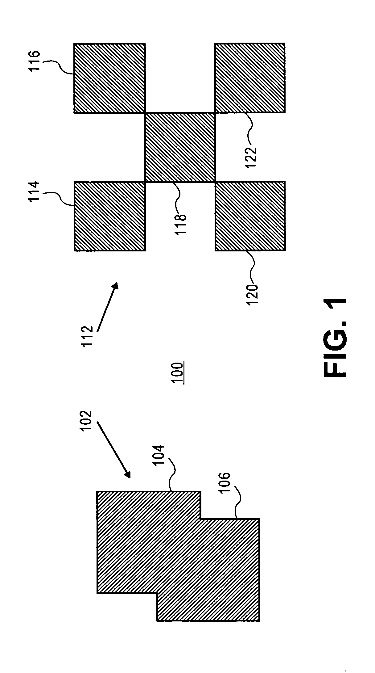
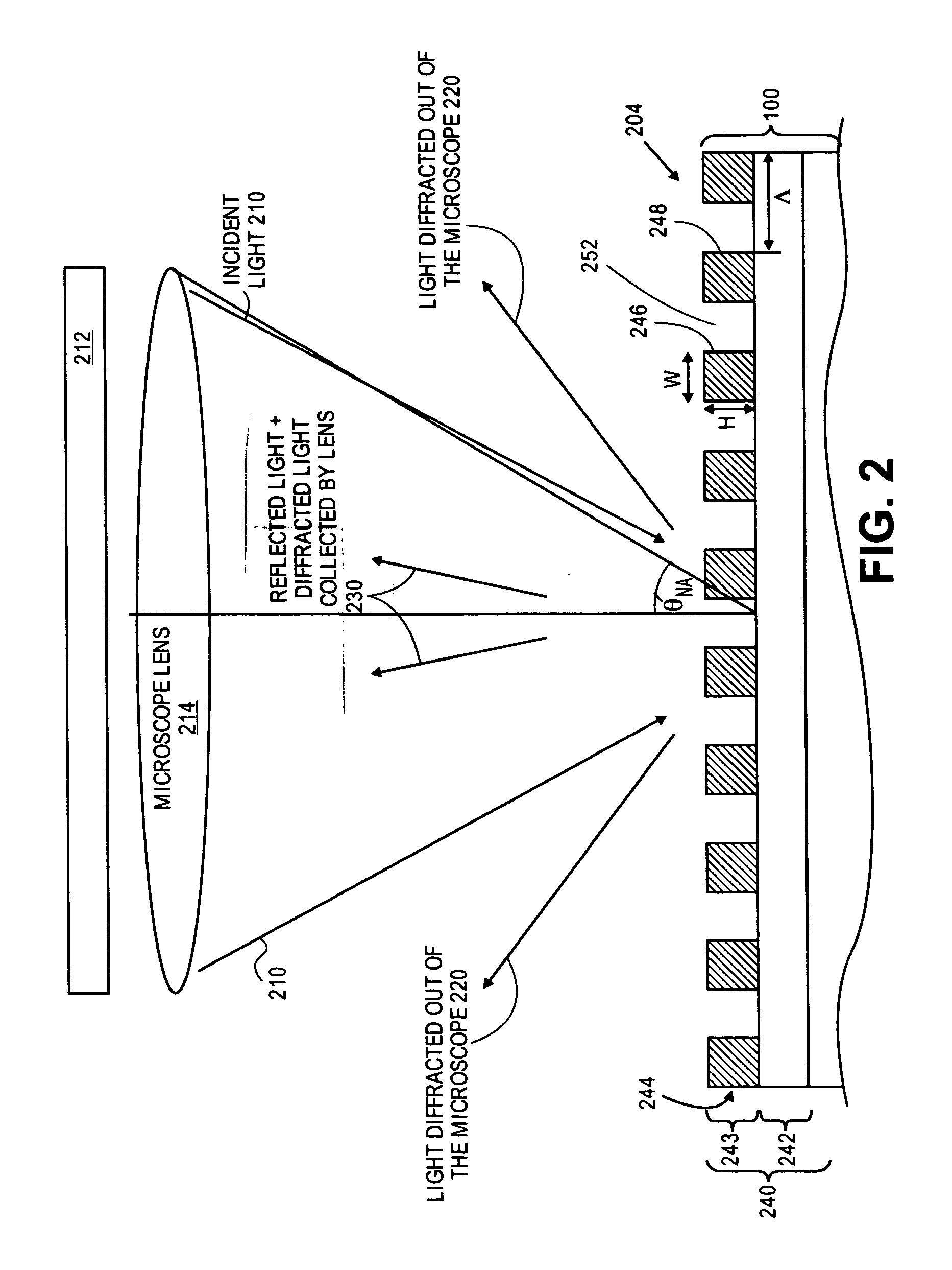
[0028]FIG. 1 is a schematic top perspective view of examples of pattern recognition targets (e.g., structures) in regions of a wafer that may be used for wafer alignment. The targets may be constructed from large patterns or structures of solid features arranged in some unique shape on or in wafer 100 (e.g., on a surface or topmost surface of wafer 100). For instance, FIG. 1 shows target 102 as a large structure having solid features 104 and 106 (e.g., solid features are not formed of gratings as mentioned below, but of solid flat layers of a single material in each region of the wafer surface).

[0029]Similarly, FIG. 1 shows target 112 as a large structure having solid features 114, 116, 118, 120, and 122. Each of features 104, 106, 114, 116, 118, 120, and 122 may be larger than the minimum resolution size (e.g., are greater than a best resolution limit possible) of a wafer alignment system inspection microscope (e.g., each of those features may be larger than a minimum size pixel th...


PUM


Abstract

Pattern recognition targets including regions of one or more layers of gratings are used for semiconductor fabrication wafer alignment. Grates of the gratings are below the resolution limit of the alignment microscopes, and have dimensions compatible with design rules applied to actual device circuitry. Targets may be located by the contrast of light 0racted back from the regions and through a numerical aperture of the microscope. Target contrast may be achieved by controlling the diffractive properties of the regions. A grating with a pitch that causes a significant amount light to diffract out of the numerical aperture will appear darker, while a grating with a pitch that produces minimal diffraction with appear much brighter. Moreover, for a darker causing pitch, a region of layers gratings having grates stacked on each other can appear even darker, while a region having layers of grates interleaved can appear even brighter.

Description

BACKGROUND[0001]1. Field[0002]Semiconductor device fabrication processing and more particularly optical pattern recognition targets for indexing wafers during device fabrication processing.[0003]2. Description of Related Art[0004]During semiconductor device fabrication processing numerous (e.g., hundreds of) integrated circuit chips or die, each having millions of electronic devices, may be formed on a single semiconductor wafer. The wafer may be a thin disk or round slice of semiconductor material (e.g., silicon), such as to provide a semiconductor (e.g., silicon, germanium, or a combination thereof) or semiconductor on insulator (SOI) substrate on or in which to form the electronic devices.[0005]Similarly, targets (e.g., wafer alignment optical targets) may be formed on or in layers of the wafer to accurately align the wafers for processing to form the devices (and to form the targets). A large number of semiconductor device fabrication processing tools perform some level of basic...

Claims


Application Information

Patent Timeline
IPC IPC(8): G01B11/14
CPCG03F9/7084G03F9/7076
Inventor WEISS, MARTIN N.
Owner INTEL CORP
Why Eureka
Try Eureka