Verification apparatus, design verification method, and computer aided design apparatus

Inactive Publication Date: 2008-01-03
FUJITSU LTD
1 Cites 5 Cited by

AI-Extracted Technical Summary

Problems solved by technology

A capacitor is a component that accumulates electricity therein, and only from that point of view, it may be utilized simply in place of a battery; however, in an electronic circuit, capacitors are scarcely utilized for that purpose.
However, it has been a problem that, when the circuit diagram becomes large-scale, the number of components and nets increases, whereby it takes a long processing time to perform the DRC.
Moreover, it has been required that the component logical types that, in the DRC, is necessary for detecting logically transparent components are manually inputted by a designer; therefore, in the case where the number of components is large, the DRC has been a cause of increase in work amount of the designer.
If the logical types of compo...

Method used

[0122]As discussed above, by, through the DRC-data creation unit 15, preliminarily creating a logically transparent ...

Benefits of technology

[0062]The present invention makes it unnecessary to detect a logically transparent component each time a DRC is performed; therefore, DRC processing time can significantly be reduced. Additionally, the present invention enables the logic types of part of or all of ...

Abstract

According to the present invention, in a CAD apparatus, circuit data for a circuit diagram created through circuit design processing is stored in a circuit database. Based on the circuit data stored in the circuit database, the respective logic types of components are discriminated and set for the component in the circuit data. Moreover, by adding logically transparent nets to the circuit data stored in the circuit database, DRC data dedicated to a DRC is created and stored in a DRC database. A DRC execution unit performs the DRC, by utilizing the DRC data stored in the DRC database.

Application Domain

Technology Topic

Computer Aided DesignCircuit design +5

Image

  • Verification apparatus, design verification method, and computer aided design apparatus
  • Verification apparatus, design verification method, and computer aided design apparatus
  • Verification apparatus, design verification method, and computer aided design apparatus

Examples

  • Experimental program(1)

Example

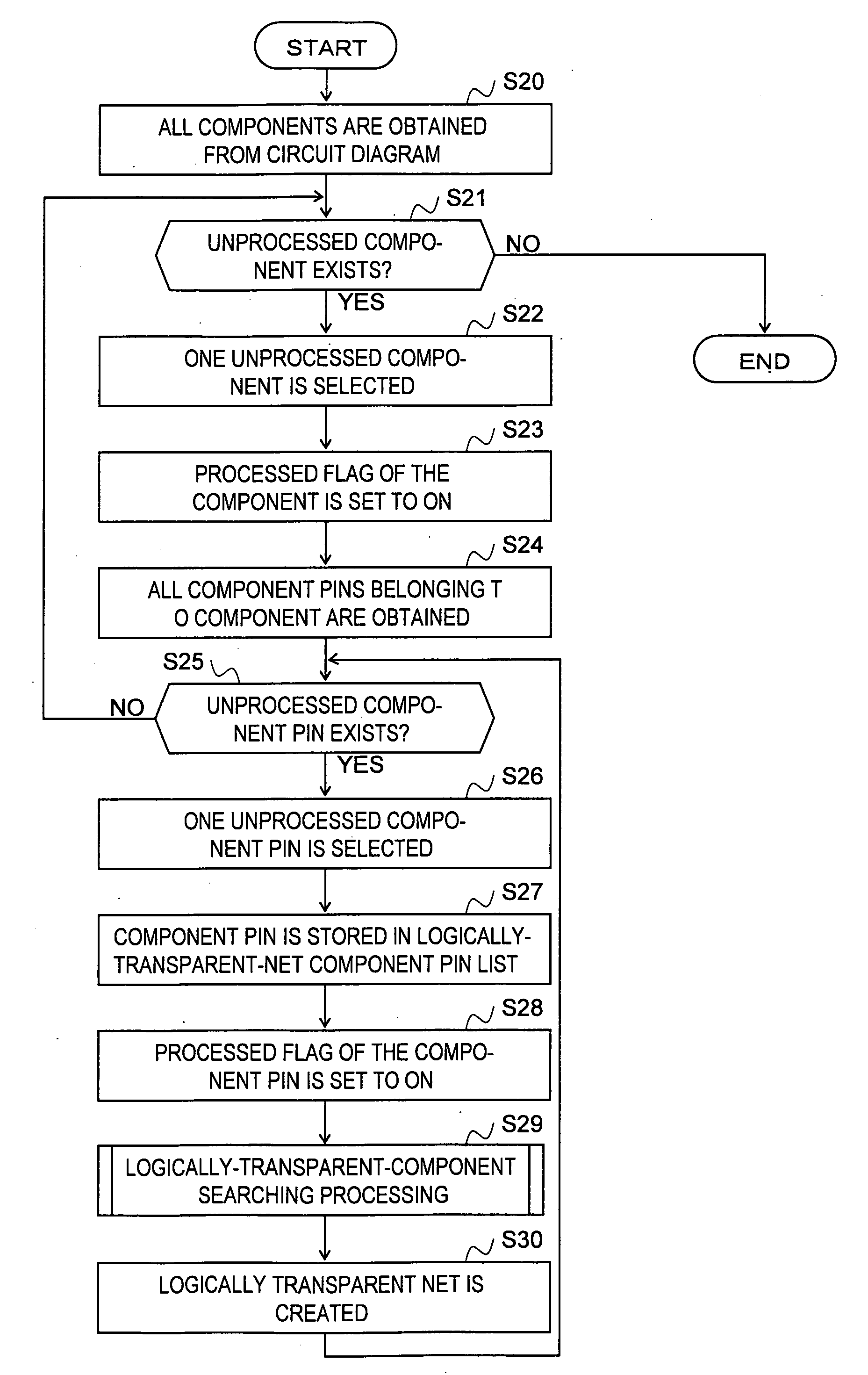
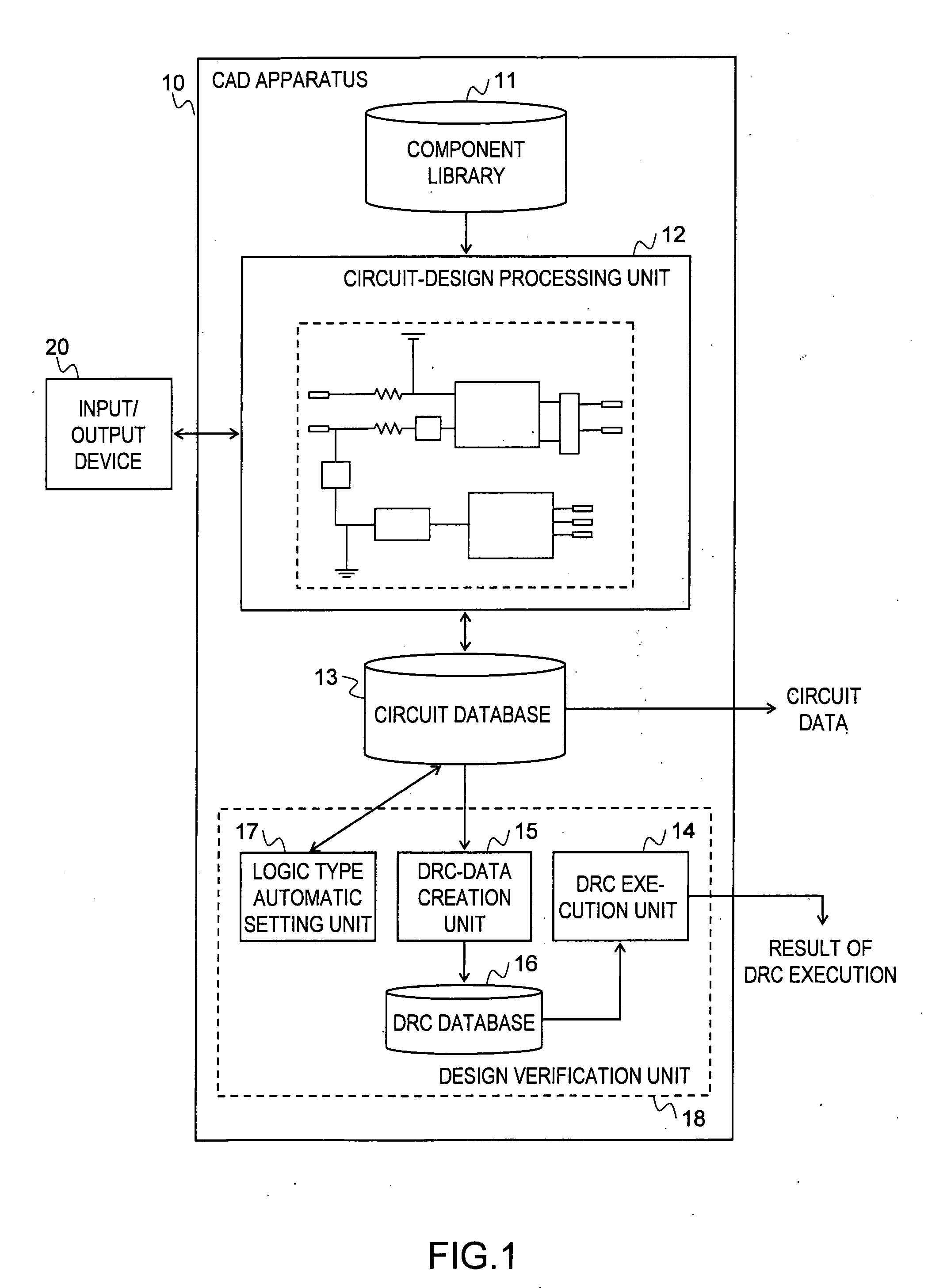
[0088]FIG. 1 is a diagram illustrating a configuration example of a CAD apparatus according to an embodiment of the present invention. A CAD apparatus 10 includes a component library 11, a circuit-design processing unit 12, a circuit database 13, a DRC execution unit 14, a DRC-data creation unit 15, a DRC database 16 and a logic type automatic setting unit 17. The DRC execution unit 14, the DRC-data creation unit 15, the DRC database 16 and the logic type automatic setting unit 17 configure a design verification unit 18 of the CAD apparatus 10 according to the present embodiment.
[0089]In response to the designer's manipulation of an input/output device 20, the circuit-design processing unit 12 carries out the processing for circuit design. By manipulating the input/output device 20, the designer selects components to be used from the component library 11 and inputs the components to a circuit diagram. The component library 11 is a library of components to be utilized in a circuit. The circuit database 13 is a database for storing the circuit data for a circuit diagram that is created by the designer. The created (or in process of creation) circuit diagram is outputted to and displayed on the input/output device 20. The processing by the circuit-design processing unit 12 is the same as that according to a conventional technique.
[0090]The DRC execution unit 14 performs the DRC on a designed circuit diagram. In the present embodiment, the DRC is performed by utilizing DRC data stored in the DRC database 16, instead of circuit data stored in the circuit database 13. In addition, in the case of a drawing check, the DRC may be performed by utilizing circuit data stored in the circuit database 13, as is the case with a conventional technique.
[0091]The DRC-data creation unit 15 creates DRC data dedicated to the DRC, based on circuit data stored in the circuit database 13. The created DRC data is stored in the DRC database 16.
[0092]The logic type automatic setting unit 17 discriminates the logic types of components in the circuit diagram, based on information, such as the types, the connection configurations, and the arrangement positions of the components, obtained from circuit data stored in the circuit database 13, and sets the obtained logic types for the corresponding components in the circuit data stored in the circuit database 13.
[0093]FIG. 2 is a diagram illustrating a configuration example of DRC data according to the present embodiment. The DRC data stored in the DRC database 16 consists of five tables, i.e., a circuit diagram table 30, a component table 31, a component pin table 32, a net table 33, and a logically transparent net table 34. The DRC data is configured in such away that the logically transparent net table 34 is added to the configuration of the circuit data illustrated in FIG. 21. The mark “*” in FIG. 2 stands for one or more pieces.
[0094]The circuit diagram table 30 is linked with a plurality of the component tables 31, a plurality of the net tables 33, and a plurality of logically transparent net tables 34. The component table 31 is linked with a plurality of the component pin tables 32 that belong thereto. The component pin table 32 is linked with a plurality of the parent component tables 31, a plurality of the connected net tables 33, and a plurality of the connected logically transparent net tables 34. The net table 33 is linked with the connected component pin tables 32. The logically transparent net table 34 is linked with the connected component pin tables 32.
[0095]FIG. 3 is a chart representing an example of the data structure of a circuit diagram table according to the present embodiment. The circuit diagram table 30 includes information on components incorporated in a printed circuit board and information on nets. The circuit diagram table 30 has information on a circuit diagram name, links to component tables, links to net tables, links to logically transparent net tables, and the like.
[0096]FIG. 4 is a chart representing an example of the data structure of a component table according to the present embodiment. The component table 31 represents components incorporated in a printed circuit board. The component table 31 has information on an ID, a component name, a processed flag, component types, logic types, links to component pin tables, and the like. The component type includes a value representing a component itself such as a resistor or a capacitor. The logic type includes a value representing the properties of a component, such as a pull-down resistor or a pull-up resistor, that is obtained by further sorting the component types. The processed flag is a flag for determining whether or not arbitrary processing has been performed.
[0097]FIG. 5 is a chart representing an example of the data structure of a component pin table according to the present embodiment. The component pin table 32 representing pins, which are connected to lines of nets, of each component. The component pin table 32 has information on an ID, a component pin name, an input/output attribution, processed flags, links to parent component tables, links to net tables, links to logically transparent net tables, and the like. The input/output attribution includes an attribution such as an input (IN), an output (OUT), or bidirectional (INOUT).
[0098]FIG. 6 is a chart representing an example of the data structure of a net table according to the present embodiment. The net table 33 represents a line of a net that connects a component with another. The net table 33 has information on an ID, a net name, a processed flag, a net attribution, links to component pin tables, and the like. The net attribution includes a value representing a net attribution such as a general net, a power source net which is connected to a power source, and an earth net which is connected to the ground.
[0099]FIG. 7 is a chart representing an example of the data structure of a logically transparent net table according to the present embodiment. The logically transparent net table 34 representing a net that passes through a logically transparent component and connects components through which the net cannot passes logically. Each net passes through a component through which the net can logically pass; therefore, the logically transparent net table 34 holds as links only the component pins of components through which nets cannot logically pass. The logically transparent net table 34 has information on an ID, a logically transparent net name, a processed flag, links to component pin tables, and the like.
[0100]FIG. 8 is a diagram for explaining the concept of a logically transparent net. FIG. 8 is an example in which a logically transparent net LT1 is set in the circuit diagram (sample) illustrated in FIG. 22. The concept of a logically transparent net is introduced in which logically permeable components are preliminarily passed through and component pins necessary for a logic check are connected with each other. In FIG. 8, a component R and a component C are logically transparent components. Accordingly, the logically transparent net LT1 eventually connects the component pin PA of the component A that is not logically permeable with the component pin PB of the component B that is not logically permeable. In addition, for convenience of explanation, FIG. 8 illustrates a logically transparent net; however, a logically transparent net is information to be set in DRC data, but not information to be set in a created circuit diagram.
[0101]FIG. 9 is a diagram illustrating an example of the structure of a DRC database for a circuit diagram. FIG. 9 is a database structure, of the DRC database 16, that represents the circuit diagram (sample) illustrated in FIG. 8. Hereinafter, a procedure for accessing a database will be explained in the case where, in the logical connection in the circuit diagram illustrated in FIG. 8, the link from the component pin PA to the component pin PB is obtained.
[0102]Procedure 1: the link from the component pin PA of the component A to the logically transparent net LT1 is obtained; and
[0103]Procedure 2: the link from the logically transparent net LT1 to the component pin PB is obtained.
[0104]As described above, by utilizing the concept of the logically transparent net, the procedure explained with reference to FIGS. 22 and 23 can significantly be reduced. The processing speed of a logical check of the DRC utilizing logically transparent nets is raised in proportion not only to the number of logically transparent components such as resistors and capacitors but also to the number of DRC check items.
[0105]FIG. 10 is a flowchart of logic check processing, carried out by the DRC execution unit, according to the present embodiment. The logic check processing carried out by the DRC execution unit 14 differs depending on the contents to be checked. Here, as is the case with FIG. 24, processing will be explained, as an example, in which whether or not any input pin exists in component pins connected to one net is checked. It is assumed that, before the start of the processing, respective processed flags for the tables are set to the initial setting values “OFF”.
[0106]In the first place, all logically transparent nets are obtained from the circuit diagram (Step S10). In other words, all the logically transparent net tables 34 that are linked with the circuit diagram table 30 are obtained. Hereinafter, it is assumed that, similarly, processing is carried out by utilizing information on the tables.
[0107]When no unprocessed (processed flag=OFF) logically transparent net exists in the logically transparent nets obtained in Step S10 (Step S11), the processing is ended.
[0108]When any unprocessed (processed flag=OFF) logically transparent net exists in the logically transparent nets obtained in Step S10 (Step S11), one unprocessed logically transparent net is selected (Step S12) and all the component-pins of the logically transparent net are obtained (Step S13).
[0109]When, after the input/output attributions of the all component pins obtained in Step S13 are ascertained, no input pin exists (Step S14), the error information on the logically transparent net selected in Step S12 is outputted (Step S15). The processed flag of the logically transparent net obtained in Step S12 is set to ON (Step S16), and then the processing in Step S11 is resumed. The error information outputted in Step S15 is, for example, an error message such as “the logically transparent net name is not connected to any input pin”.
[0110]In the present embodiment, an example of a check on the existence of an input pin has been explained; however, a check on whether or not any unconnected power supply pin remains, a check on whether or not no output pin exists in a net, a check on dot logic, and the like can also be carried out at high speed, by utilizing the logically transparent net.
[0111]Next, the creation processing, of a logically transparent net, by the DRC-data creation unit 15 will be explained. Here, in the first place, an example of a specific processing procedure will be explained with reference to an example of a circuit diagram in FIG. 8. It is assumed that, before the start of the following processing, respective processed flags for the tables are set to the initial setting values “OFF”.
[0112]Procedure 1: the components (the component A, the component B, the component R, and the component C) are obtained from the sample circuit diagram;
[0113]Procedure 2: at this time point, the component A, the component B, the component R, and the component C are all unprocessed (processed flag=OFF) components; it is found that, from the respective logic types of the obtained components, the component R and the component C are logically transparent components; here, it is assumed that the component A, out of the component A and the component B that are not logically transparent components, is selected and the processing is started with the component A;
[0114]Procedure 3: the component pin PA of the component A is obtained; because the component A is not a logically transparent component, the component pin PA is stored in a logically-transparent-net component pin list; the processed flag of the component PA is set to ON; here, the logically-transparent-net component pin list is a list for the component pins connected to a logically transparent net to be created;
[0115]Procedure 4: the net N1 connected to the component pin PA is obtained;
[0116]Procedure 5: the link from the net N1 to the component pin PR1 is obtained (because the component pin PA has been processed); the processed flag of the component pin PR1 is set to ON;
[0117]Procedure 6: because the component R that is the parent component of the component pin PR1 is a logically transparent component, the component pin PR1 is not added to the logically-transparent-net component pin list; the link from the component R to the component pin PR2 is obtained (because the component pin PR1 has been processed); the processed flag of the component pin PR2 is set to ON;
[0118]Procedure 7: the link from the component pin PR2 to the net N2 is obtained;
[0119]Procedure 8: because, as is the case with the component R, the component C is a logically transparent component, the following processing that is the same as that from the procedure 5 to the procedure 7 is carried out so as to obtain the net N3.
[0120]Procedure 9: the link from the net N3 to the component pin PB is obtained; because the component B that is the parent component of the component pin PB is not a logically transparent component, the component pin PB is stored in a logically-transparent-net component pin list; and
[0121]Procedure 10: finally, the component pins PA and PB of the components A and B, respectively, that are not logically transparent components are stored in the logically-transparent-net component pin list; the logically transparent net LT1 is created and the links to component pins PA and PB are set.
[0122]As discussed above, by, through the DRC-data creation unit 15, preliminarily creating a logically transparent net for the whole circuit, the logic check processing by the DRC execution unit 14 can be carried out at high speed.
[0123]FIG. 11 is a flowchart of logically-transparent-net creation processing, carried out by the DRC execution unit, according to the present embodiment. It is assumed that, before the start of the processing, respective processed flags for the tables are set to the initial setting values “OFF”.
[0124]In the first place, all components are obtained from the circuit diagram (Step S20). In other words, all the component tables 31 that are linked with the circuit diagram table 30 are obtained. Hereinafter, it is assumed that, similarly, processing is carried out by utilizing information on the tables.
[0125]When no unprocessed (processed flag=OFF) component exists in the components obtained in Step S20 (Step S21), the processing is ended.
[0126]When any unprocessed (processed flag=OFF) component exists in the components obtained in Step S20 (Step S21), one unprocessed component is selected (Step S22), the processed flag of the component is set to ON (Step S23) and all the component pins belonging to the component are obtained (Step S24). In addition, when an unprocessed component is selected, logic types are ascertained so as to select a component that is not a logically transparent component.
[0127]When no unprocessed (processed flag=OFF) component pin exists in the component pins obtained in Step S24 (Step S25), the processing in Step S21 is resumed.
[0128]When any unprocessed (processed flag=OFF) component pin exists in the component pins obtained in Step S24 (Step S25), one unprocessed component pin is selected (Step S26), the component pin is stored in a logically-transparent-net component pin list (Step S 27) and the processed flag of the component pin is set to ON (Step S28). Logically-transparent-component searching processing, described later, is carried out (Step S29). Based on the logically-transparent-net component pin list, a logically transparent net is created (Step S30). In other words, the logically transparent net table 34 is created that has a link with the table for the component pin stored in the logically-transparent-net component pin list. In addition, each time the logically transparent net table 34 is created, the logically-transparent-net component pin list is cleared. The processing in Step S25 is resumed.
[0129]FIG. 12 is a flowchart illustrating the logically-transparent-component searching processing. With a component pin considered as an input, the logically-transparent-component searching processing is carries out.
[0130]In the first place, all nets connected to the obtained (or selected) component pin are obtained (Step S40). All the component pins connected to the obtained net are obtained (Step S41).
[0131]When no unprocessed (processed flag=OFF) component pin exists in the component pins obtained in Step S41 (Step S42), the processing is ended.
[0132]When any unprocessed (processed flag=OFF) component pin exists in the component pins obtained in Step S41 (Step S42), one unprocessed component pin among component pins that are obtained in Step S41 is selected (Step S43), the processed flag of the selected component pin is set to ON (Step S 44).
[0133]When the parent component of the component pin selected in Step S43 is a logically transparent component (Step S45), the processed flag of the parent component of the component pin selected in Step S43 is set to ON (Step S46). The component pin, of the parent component, opposite to the component pin selected in Step S43 is obtained (Step S47), and the processed flag of the component pin obtained in Step S47 is set to ON (Step S48). The logically-transparent-component searching processing is recursively carried out (Step S49). The processing in Step S42 is resumed. In addition, whether or not a component is a logically transparent component is determined based on the component logical type and the like.
[0134]When the parent component of the component pin selected in Step S43 is not a logically transparent component (Step S45), the component pin selected in Step S43 is stored in the logically-transparent-net component pin list (Step S50) and the processing in Step S42 is resumed.
[0135]Next, automatic setting of the logic types of components will be explained. In the case where a logically transparent net is created by the DRC-data creation unit 15, it is required that the respective logic types of components have been set so that whether or not each component is a logically transparent component is determined. In the present embodiment, the logic type automatic setting unit 17 automatically discriminates the logic types of components in the circuit diagram, based on information, such as the types, the connection configurations, and the arrangement positions of the components, obtained from circuit data stored in the circuit database 13, and sets the obtained logic types of the components in the component tables for the circuit data stored in the circuit database 13. In addition, all the respective logic types of components may automatically be set or it may also possible that part of the logic types are automatically set and the rest is manually set by a designer.
[0136]The logically transparent components are various components including a dumping resistor and a coupling capacitor described above. Here, as examples, five logically transparent resistors will be explained with reference to the drawings.
[0137]FIG. 13 is a diagram for explaining a pull-down resistor. A resistor that has two terminals the one of which is connected to a general net and the other of which is connected to the earth net is referred to as a pull-down resistor.
[0138]FIG. 14 is a diagram for explaining a pull-up resistor. A resistor that has two terminals the one of which is connected to a general net and the other of which is connected to the power-source net is referred to as a pull-up resistor.
[0139]FIG. 15 is a diagram for explaining a thevenin resistor. In the case where the pull-down resistor illustrated in FIG. 13 and the pull-up resistor illustrated in FIG. 14 exist in the same net, the combination of both resistors is referred to as a thevenin resistor.
[0140]FIG. 16 is a diagram for explaining a dumping resistor. A resistor that has two terminals that are each connected to a general net is referred to as a dumping resistor.
[0141]FIG. 17 is a diagram for explaining a differential termination resistor. A resistor that has two terminals that are each connected to a net set as a balanced transmission path is referred to as a differential termination resistor.
[0142]As described above, the conditions for determining the respective logic types of components are clear; therefore, by analyzing information obtained from circuit data stored in the circuit database 13, the logic types of components can automatically be discriminated and set. For example, in the case where the component type, in the component table 31, of a component is a resistor, the component has links with two component pin tables 32, one of the component pin tables 32 has a link to a net table 33 whose net attribution is an earth net, and the other of the component pin tables 32 has a link to a net table 33 whose net attribution is a general net, it can readily be determined that the component is a pull-down resistor.
[0143]FIG. 18 is a flowchart of logic type automatic setting processing, carried out by a logic type automatic setting unit, according to the present embodiment. In the present embodiment, an example will be described in which the logic types of a pull-down resistor, a pull-up resistor, and a dumping resistor, which are readily discriminated, are automatically set. Similarly, the discrimination processing logic corresponding to each logic type enables the logic-type automatic setting of components of other logic types. It is assumed that, before the start of the processing, respective processed flags for the tables are set to the initial setting values “OFF”.
[0144]In the first place, all components are obtained from the circuit diagram (Step S60). In other words, all the component tables 31 that are linked with the circuit diagram table 30 are obtained. Hereinafter, it is assumed that, similarly, processing is carried out by utilizing information on the tables.
[0145]When no unprocessed (processed flag=OFF) component exists in the components obtained in Step S60 (Step S61), the processing is ended.
[0146]When any unprocessed (processed flag=OFF) component exists in the components obtained in Step S60 (Step S61), one unprocessed component is selected (Step S62) and the processed flag of the selected component is set to ON (Step S 63).
[0147]When the component type of the component selected in Step S62 is not a resistor (Step S64), or the number of the links, of the component selected in Step S62, to component pins is not two (Step S65), the processing in Step S61 is resumed.
[0148]When the component type of the component selected in Step S62 is a resistor (Step S64) and the number of the links, of the component selected in Step S62, to component pins is two (Step S65), the two component pins of the selected component are obtained (Step S66). Respective nets connected to the two component pins obtained in Step S66 are obtained (Step S67).
[0149]When the net attributions of the two nets obtained in Step S67 are both general nets (Step S68), a dumping resistor is set in the logical type of the component selected in Step S62 (Step S69) and the processing in Step S61 is resumed.
[0150]When one of the net attributions of the two nets obtained in Step S67 is a general net and the other is an earth net (Step S70), a pull-down resistor is set in the logical type of the component selected in Step S62 (Step S71) and the processing in Step S61 is resumed.
[0151]When one of the net attributions of the two nets obtained in Step S67 is a general net and the other is a power-source net (Step S72), a pull-up resistor is set in the logical type of the component selected in Step S62 (Step S73) and the processing in Step S61 is resumed.
[0152]When the logic type is none of a pull-down resistor, a pull-up resistor, and a dumping resistor, the processing in Step S61 is directly resumed.
[0153]As illustrated in FIG. 18, the respective logic types of components can automatically be set, by discriminating them, based on the information on tables in circuit data stored in the circuit database 13. Additionally, instead of automatically setting the logic types of all components, the logic types of part of all the components may manually be set.
[0154]The processing related to the design verification according to the present embodiment described above can be realized by means of a computer and a software program; it is possible not only to store the program in a computer readable storage medium, but also to provide the program through a network.
[0155]An embodiment of the present invention has been explained heretofore; however, the present invention is not limited thereto. For example, in the present embodiment, an example has been described in which the present invention is applied to design verification in the circuit design (P12) illustrated in FIG. 19; however, the present invention can readily be applied to design verification in the mounting design (P14) illustrated in FIG. 19.

PUM

no PUM

Description & Claims & Application Information

We can also present the details of the Description, Claims and Application information to help users get a comprehensive understanding of the technical details of the patent, such as background art, summary of invention, brief description of drawings, description of embodiments, and other original content. On the other hand, users can also determine the specific scope of protection of the technology through the list of claims; as well as understand the changes in the life cycle of the technology with the presentation of the patent timeline. Login to view more.

Similar technology patents

Classification and recommendation of technical efficacy words

  • Reduce processing time
  • Reduce time

Multi-component vascular device

ActiveUS20090099647A1Reduce timeReduce inventoryStentsDiagnosticsBody organsTreating Site
Owner:ST JUDE MEDICAL CARDIOLOGY DIV
Why Eureka
Try Eureka