DC Offset Cancellation For A Trans-Impedance Amplifier

a trans-impedance amplifier and offset cancellation technology, which is applied in the direction of amplifiers, amplifiers with semiconductor devices only, amplifiers with semiconductor devices, etc., can solve the problems of 40 db difference between low and high values, 100 times more difficult and expensive to integrate on-chip

Active Publication Date: 2008-01-10
LUMENTUM OPERATIONS LLC
View PDF9 Cites 25 Cited by
  • Summary
  • Abstract
  • Description
  • Claims
  • Application Information

AI Technical Summary

Problems solved by technology

Unfortunately, the photodiode DC current IPD can vary from about 10 uA up to about 1000 uA, which makes a 40 dB of difference between the low and high

Method used


Image

  • DC Offset Cancellation For A Trans-Impedance Amplifier
  • DC Offset Cancellation For A Trans-Impedance Amplifier
  • DC Offset Cancellation For A Trans-Impedance Amplifier

Examples


Embodiment Construction

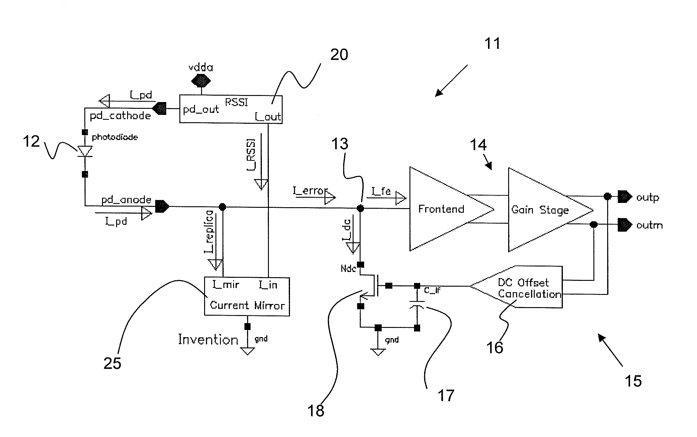
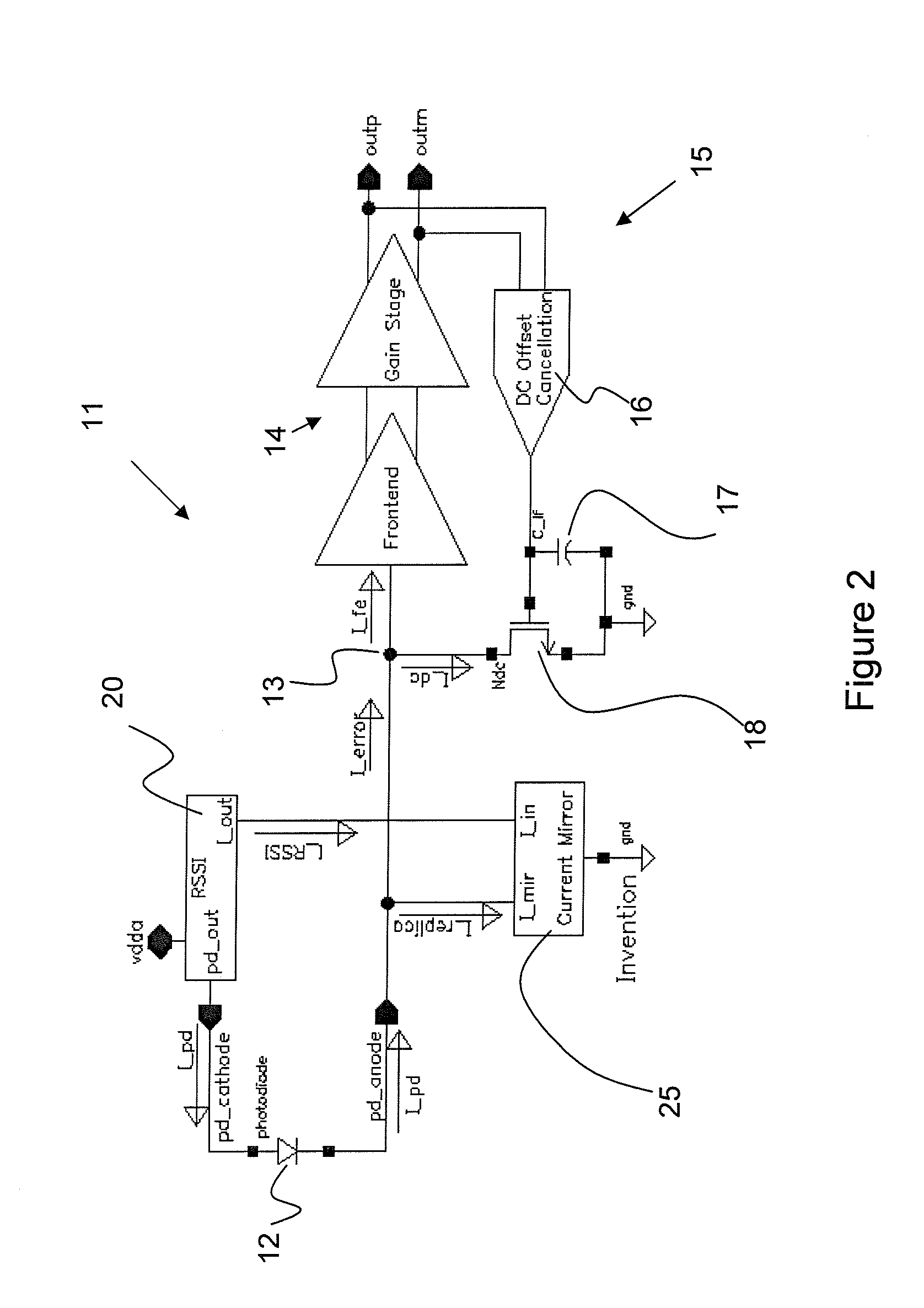
[0014]The present invention solves the aforementioned problem by using the output current from a photodiode monitoring circuit, e.g. a Receive Signal Strength Indicator (RSSI), to cancel the dc offset current from the photodiode before entering the trans-impedance amplifier (TIA). As illustrated in FIG. 2, a TIA circuit 11 receives photodiode current IPD from a photodetector, e.g. photodiode 12, via input terminal 13, and converts the photodiode current IPD to a voltage that is further amplified by an amplification chain 14, thereby producing a differential output voltage VOUT=Outp-Outn.

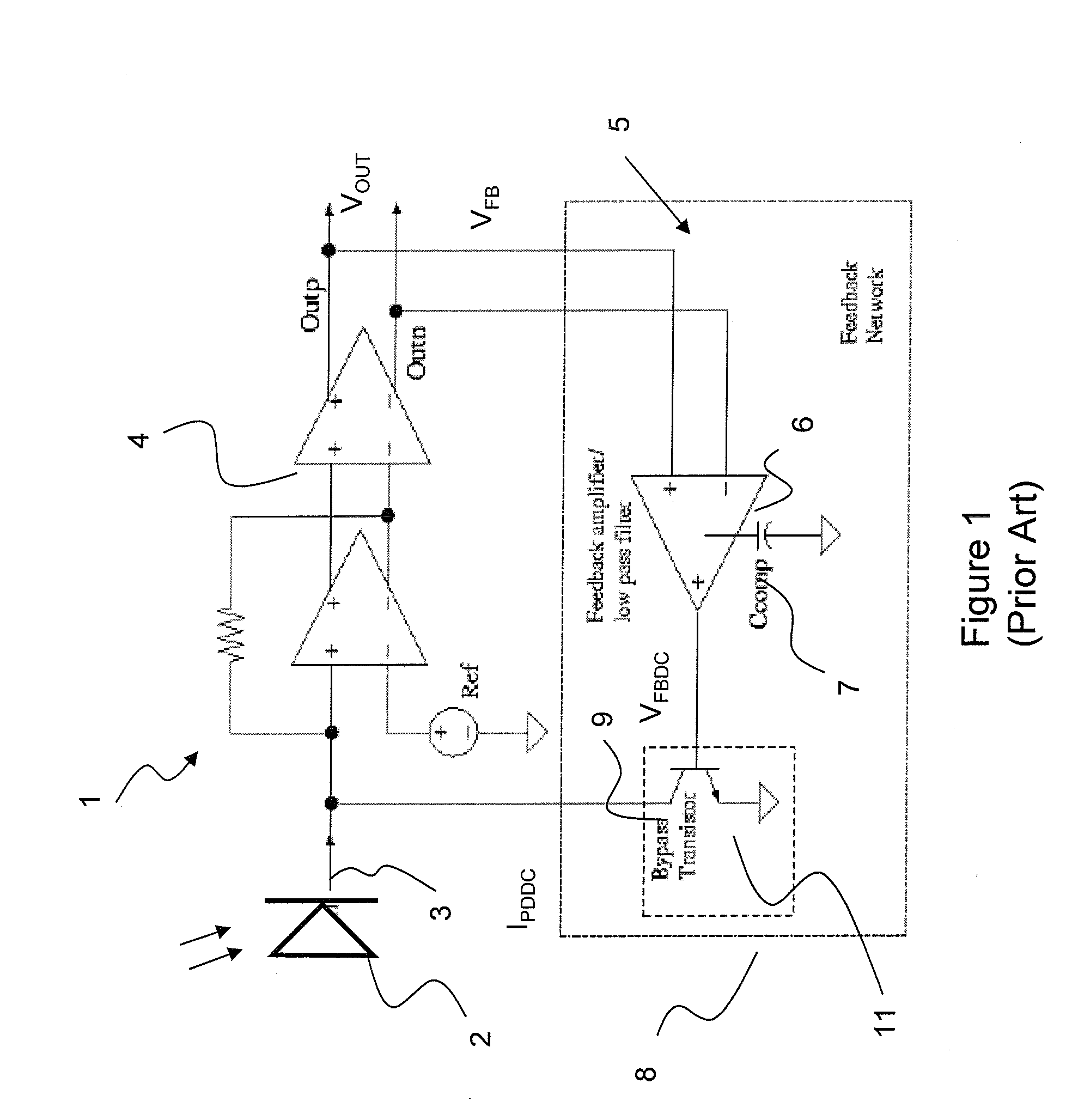
[0015]Conventional DC offset cancellation is accomplished by a feedback network 15 including a feedback amplifier 16 / low pass capacitor filter 17, and bypass transistor 18 combination, as hereinbefore discussed, integrated on a integrated circuit chip; however other means of DC offset cancellation are possible within the scope of this invention.

[0016]A photocurrent monitor function provides a DC sign...


PUM


Abstract

The invention relates to a DC offset cancellation circuit for a trans-impedance amplifier, which is typically used for converting an input current from a photodiode into an output voltage. The DC offset cancellation circuit utilizes the monitor current from a photodiode monitoring device to cancel the DC offset from the photodiode input current, enabling the conventional feedback circuit in the trans-impedance amplifier to be fully integrated.

Description

CROSS-REFERENCE TO RELATED APPLICATIONS[0001]The present invention claims no priority.TECHNICAL FIELD[0002]The present invention relates to a circuit for canceling or reducing DC offset current from a photodiode, and in particular to the use of an existing power monitor circuit to subtract the bulk of the photodiode DC offset current ahead of and independent of the DC cancellation feedback loop to reduce the burden on the offset cancellation circuit.BACKGROUND OF THE INVENTION[0003]A level restoration circuit in a trans-impedance amplifier removes the DC component, i.e. the average value which carries no information, of an optical signal exiting an optical fiber onto a photodiode in a receiver optical sub-assembly (ROSA), while at the same time keeping the low frequency −3 dB frequency low enough to meet requirements for both Telecom and Datacom applications.[0004]With reference to FIG. 1, a conventional TIA circuit, generally indicated at 1, converts the current IPD exiting a photo...

Claims


Application Information

Patent Timeline
IPC IPC(8): H03F3/08
CPCH03F3/08H03G3/3084H03F2200/375H03F3/45941
Inventor NATZKE, BRAD ANTHONY
Owner LUMENTUM OPERATIONS LLC
Why Eureka
Try Eureka