Semiconductor device

a technology of semiconductors and circuits, applied in the direction of power supply for data processing, near-field systems using receivers, instruments, etc., can solve the problems of reducing the size of transistors and layout areas, further difficulty in designing regulator circuits, and reducing power consumption in the regulator circuit. , the effect of reducing the size of the transistor and a layout area

Inactive Publication Date: 2008-01-17
SEMICON ENERGY LAB CO LTD
View PDF32 Cites 45 Cited by
  • Summary
  • Abstract
  • Description
  • Claims
  • Application Information

AI Technical Summary

Benefits of technology

[0026]Thus, although in the second regulator circuit, the first function is used to suppress the first fluctuation and the second function is used to suppress the second fluctuation caused in the second circuit, the design of the second regulator circuit is not necessarily as complicated as the first regulator circuit. That is, in the second regulator circuit, a size of the transistor and a layout area can be reduced as compared to the

Problems solved by technology

Therefore, if clock frequency fluctuates in operation, the RFID cannot accurately interpret a command or data each from the reader-writer to the RFID.
In addition, if clock frequency fluctuates in operation, the reader-writer cannot accurately interpret a response from the RFID to the reader-writ

Method used


Image

  • Semiconductor device
  • Semiconductor device
  • Semiconductor device

Examples


embodiment mode 1

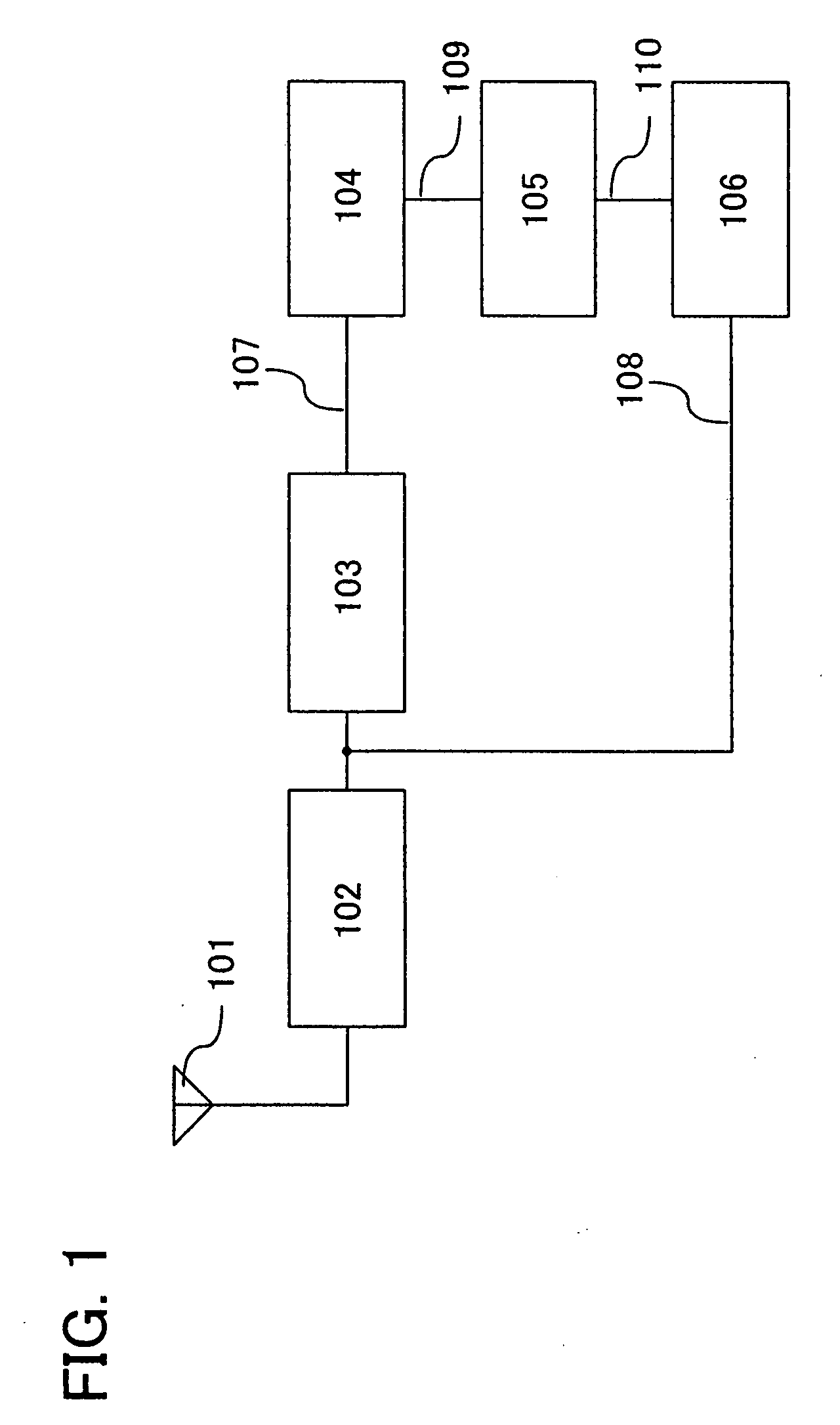
[0046]A structure of an RFID of the present invention is shown by a block diagram in FIG. 1.

[0047]The RFID shown in FIG. 1 includes an antenna 101, a rectifier circuit 102, a regulator circuit 103, a first circuit 104, a level shifter circuit 105, and a second circuit 106. The antenna 101 and the rectifier circuit 102 generate a power source potential needed for the first circuit 104 and the second circuit 106 from a radio wave or an electromagnetic wave, that is, a wireless signal (also referred to as a communication signal) from a reader-writer, which is received by the antenna 101. Actually, a signal is extracted from the antenna 101, the signal is processed by the second circuit 106, and a result of the process by the second circuit 106 is transmitted to the reader / writer from the antenna 101.

[0048]The first circuit 104 is a circuit that needs a given stable power source potential like a clock generating circuit, and the second circuit 106 is a circuit other than the circuit tha...

embodiment mode 2

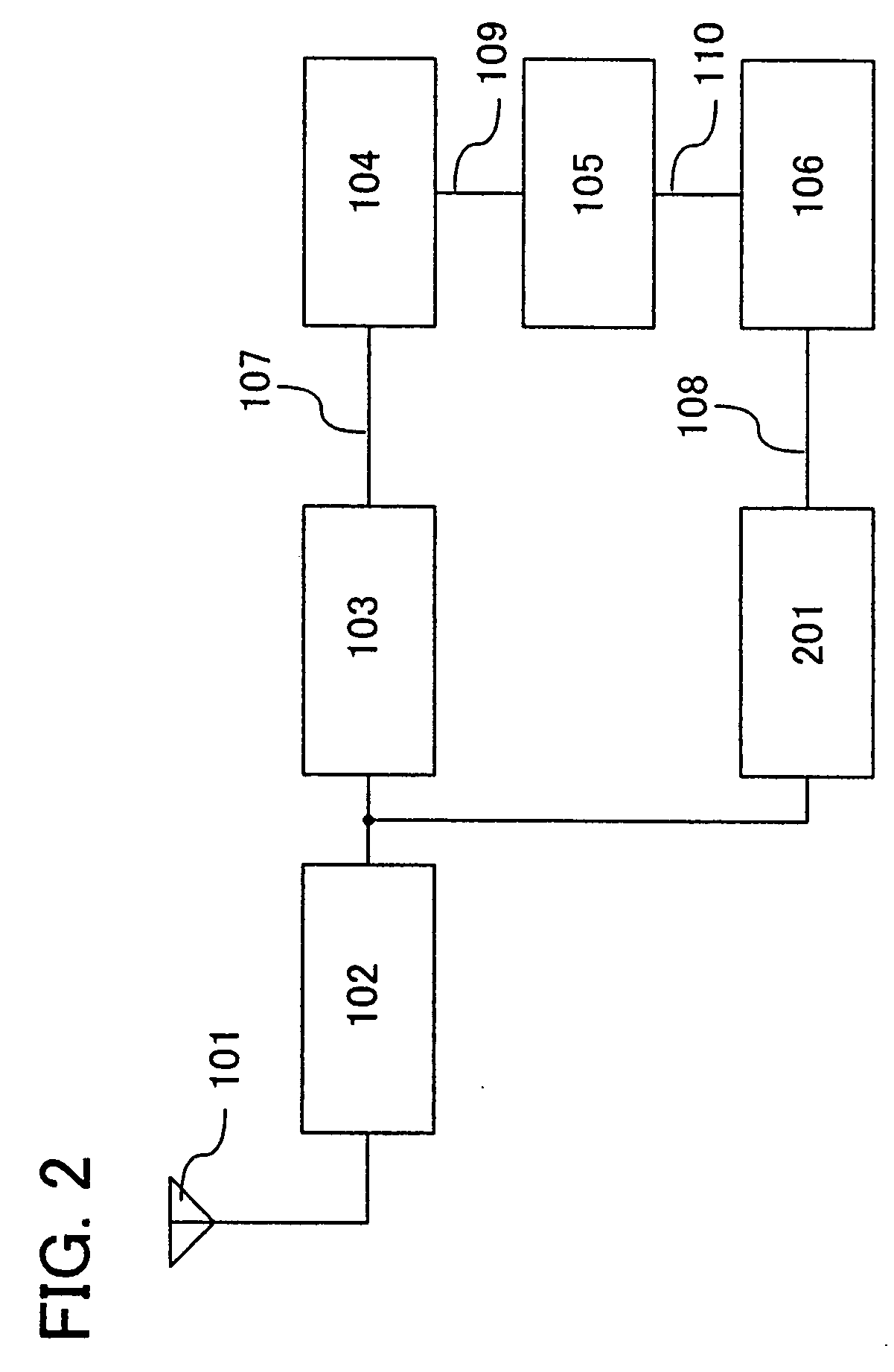
[0070]In this embodiment mode, a structure of another mode than Embodiment Mode 1 is described with reference to FIG. 2. Note that the RFID shown in FIG. 2 has a structure in which the regulator circuit 201 is added to the structure of the RFID shown in FIG. 1 and includes the antenna 101, the rectifier circuit 102, the regulator circuit 103, the first circuit 104, the level shifter circuit 105, the second circuit 106, and the regulator circuit 201. Note that similar portions to those in FIG. 1 are denoted by the same reference numerals in FIG. 2, and description thereof is omitted. In addition, in order to distinguish the regulator circuit 103 and the regulator circuit 201, they are respectively referred to as a first regulator circuit and a second regulator circuit.

[0071]In FIG. 2, the regulator circuit 201 prevents a power source potential of the second circuit 106 from being too high. A state where a power source potential of the second circuit 106 is too high corresponds to a s...

embodiment mode 3

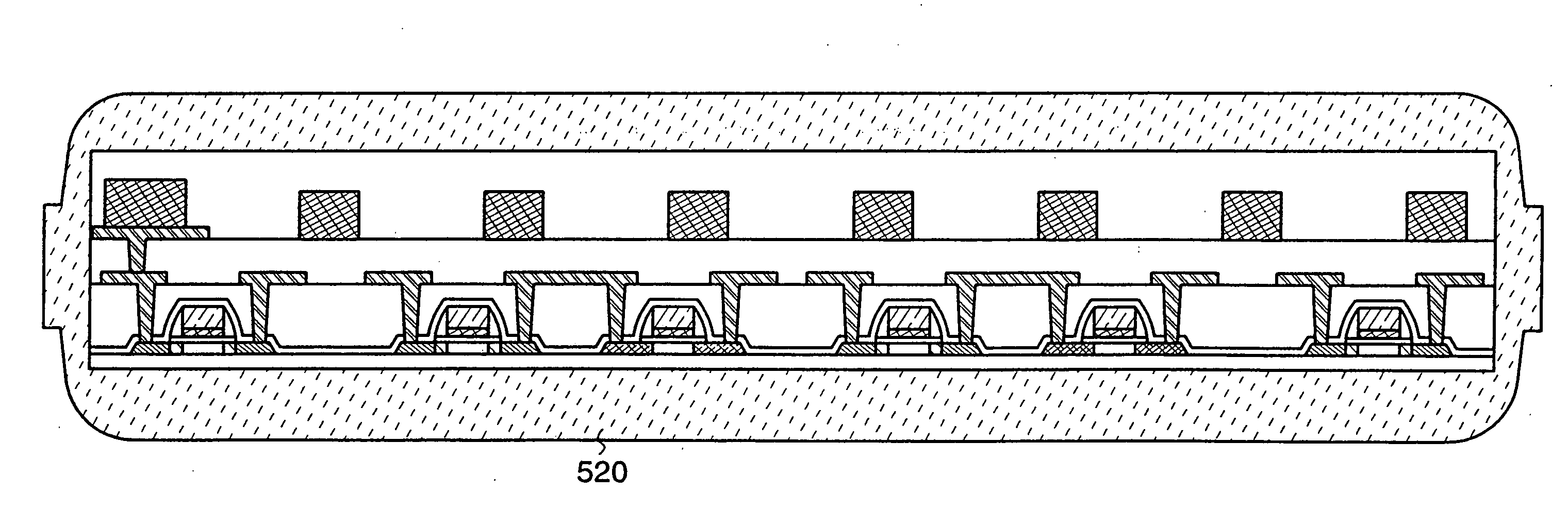
[0077]In this embodiment mode, an example of a method for manufacturing the semiconductor device such as an RFID described in the aforementioned embodiment mode is described with reference to partial cross-sectional views.

[0078]First, as shown in FIG. 5A, a release layer 503 is formed over one side of the substrate 501 with an insulating film 502 interposed therebetween. Subsequently, an insulating film 504 that function as base film and a semiconductor film 505 (for example, a film containing amolphous silicon) are stacked. Note that the insulating film 502, the release layer 503, the insulating film 504, and the semiconductor film 505 can be sequentially formed.

[0079]As the substrate 501, a glass substrate, a quartz substrate, a metal substrate (such as a stainless steel substrate), a ceramic substrate, or a semiconductor substrate such as a silicon substrate can be used. Alternatively, a substrate formed of polyethylene terephthalate (PET), polyethylene naphthalate (PNT), polyeth...


PUM


Abstract

A semiconductor device such as an RFID, which can easily generate a given stable potential, is provided. Circuits included in a semiconductor device are categorized depending on whether a given stable power source potential is necessary. A power source potential generated from a wireless signal received by an antenna with the use of the antenna and a rectifier circuit is supplied to a circuit which needs a given stable power source potential through a regulator. On the other hand, a power source potential generated by the rectifier circuit is supplied to a circuit other than the circuit which needs the arbitrary power source potential. Thus, a semiconductor device including a regulator circuit easily designed with a smaller layout can be provided, and the semiconductor device can easily generate a given stable power source potential.

Description

BACKGROUND OF THE INVENTION[0001]1. Field of the Invention[0002]The present invention relates to a semiconductor device such as an RFID formed over a glass substrate or a flexible substrate. The present invention also relates to a semiconductor device which performs communication without contact.[0003]2. Description of the Related Art[0004]In recent years, an individual identification technology using wireless communication through an electromagnetic field, a radio wave, or the like has attracted attention. In particular, as a semiconductor device which communicates data by wireless communication, an individual identification technology using an RFID (Radio Frequency Identification) tag has attracted attention. An RFID tag (hereinafter, simply referred to as an RFID) is also called an IC (Integrated Circuit) tag, an RF tag, a wireless tag, an electronic tag, an IC chip, or a wireless chip. The individual identification technology using an RFID has come to help production, management...

Claims


Application Information

Patent Timeline
IPC IPC(8): G06K19/06
CPCG06F1/189G06K19/07749G06F1/26H04B5/02
Inventor IKEDA, TAKAYUKIKUROKAWA, YOSHIYUKIENDO, MASAMI
Owner SEMICON ENERGY LAB CO LTD
Why Eureka
Try Eureka