

Metal-oxide-semiconductor transistor device, manufacturing method thereof, and method of improving drain current thereof
a technology of metal-oxide-semiconductor transistor and manufacturing method, which is applied in the direction of semiconductor devices, basic electric elements, electrical appliances, etc., can solve the problems of limited photolithography, the channel width still depends on and is limited to the ultimate size of the device obtained, and the inability to increase the driving current of the mos transistor, etc., to achieve the effect of improving the drain current and improving the channel width of the metal-oxide-semiconductor transistor
- Summary
- Abstract
- Description
- Claims
- Application Information
AI Technical Summary
Benefits of technology
Problems solved by technology
Method used
Image

Examples
Embodiment Construction
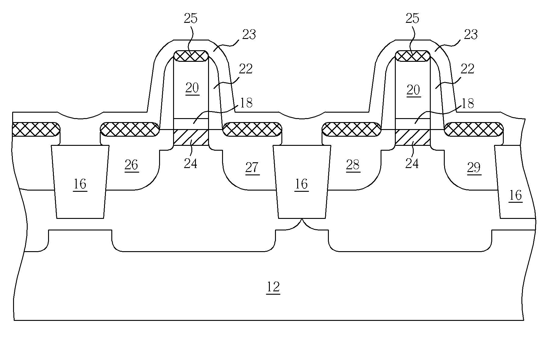
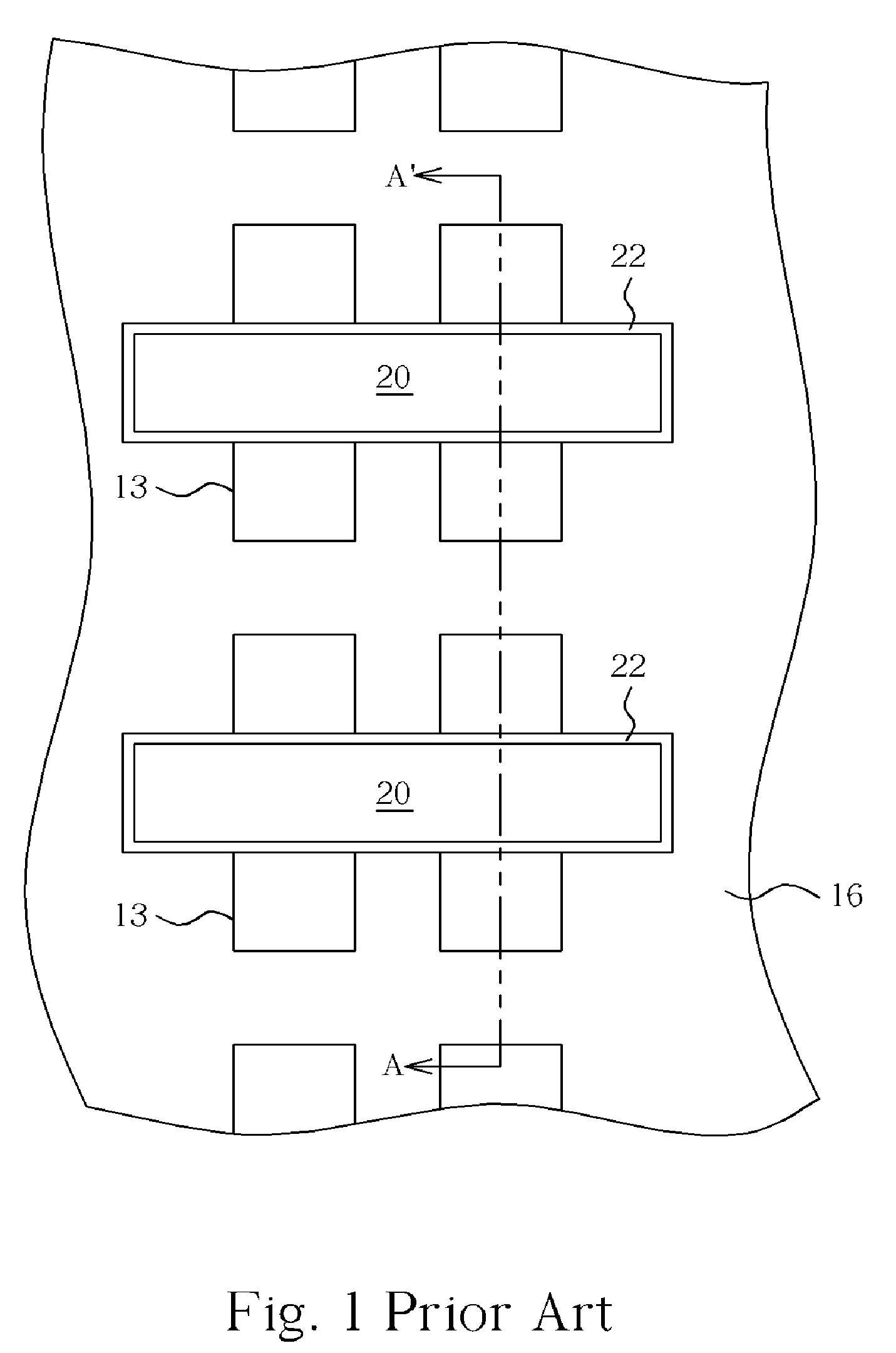
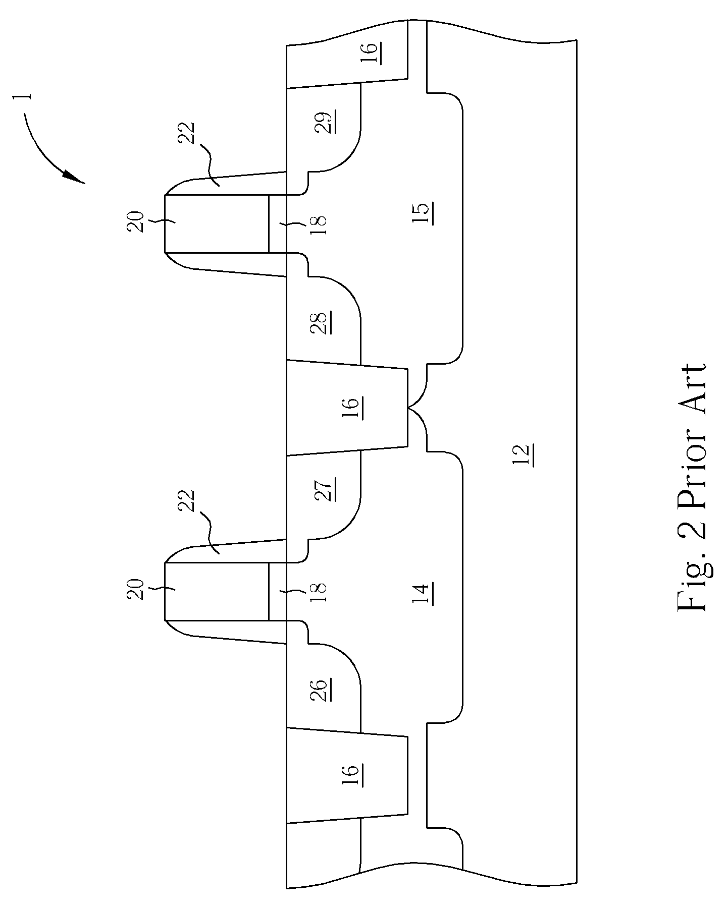
[0029]The metal-oxide-semiconductor transistor device according to the present invention may be an NMOS, a PMOS, or a CMOS transistor device. FIG. 4 shows a schematic top-view diagram of a plurality of the MOS transistor device according to the present invention. FIG. 5 shows a schematic cross-section view diagram taken along the line BB′ in FIG. 4. The description is referred to a CMOS transistor device structure. Like number numerals designate similar or the same parts, regions or elements. It is to be understood that the drawings are not drawn to scale and are served only for illustration purposes. CMOS transistor device 10 comprises a semiconductor substrate. The semiconductor substrate comprises an active region 13 and an insulation region 16 surrounding the active region 13 for electric insulation. A gate structure comprising, for example, a gate insulation layer 18, a gate electrode layer 20, and a spacer 22, is disposed on the active region 13. The epitaxial layer 24 is betw...
PUM
 Abstract
Description
Claims
Application Information