Si-substrate and structure of opto-electronic package having the same
- Summary
- Abstract
- Description
- Claims
- Application Information
AI Technical Summary
Benefits of technology
Problems solved by technology
Method used
Image
Examples
Embodiment Construction
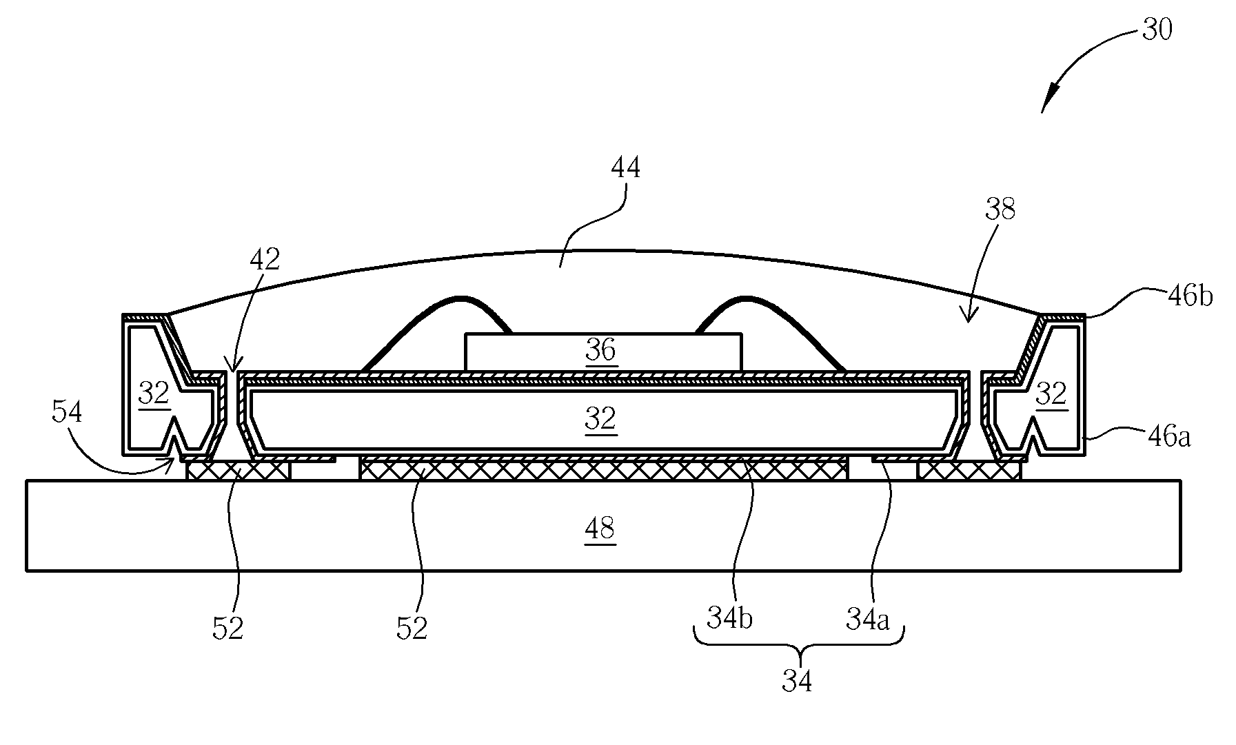
[0017]Please refer to FIG. 3 and FIG. 4. FIG. 3 is a schematic cross-sectional diagram illustrating an opto-electronic package structure 30 having a Si-substrate 32 according to a first preferred embodiment of the present invention, and FIG. 4 is a schematic top view of the opto-electronic package structure 30 shown in FIG. 3. It is to be understood that the drawings are not drawn to scale and are used only for illustration purposes. As shown in FIG. 3 and FIG. 4, an opto-electronic package structure 30 includes a Si-substrate 32, a plurality of connecters 34 and at least an opto-electronic device 36. The material of the Si-substrate 32 includes polysilicon, amorphous silicon or single-crystal silicon. In addition, the Si-substrate 32 can be a rectangle silicon chip or a circular silicon chip, and can include integrated circuits or passive components therein. The Si-substrate 32 has a top surface and a bottom surface. A cup-structure 38 can be included on the top surface of the Si-s...
PUM
 Abstract
Description
Claims
Application Information


