Compliant Bumps for Integrated Circuits Using Carbon Nanotubes

a technology of integrated circuits and carbon nanotubes, which is applied in the direction of electrical equipment, semiconductor devices, semiconductor/solid-state device details, etc., can solve the problems of lowering the amplification capabilities of amplifiers, high-frequency, high-power amplifiers, etc., and presenting a host of problems for circuit designers

Inactive Publication Date: 2008-01-24
APPLIED NANOTECH HLDG
View PDF6 Cites 9 Cited by
  • Summary
  • Abstract
  • Description
  • Claims
  • Application Information

AI Technical Summary

Problems solved by technology

High-frequency, high-power (e.g., amplifiers) present a host of problems for circuit designers.
However, as high-power amplifiers began to function at increasingly higher frequencies, the use of such connecting wired proved problematic.
For instance, the connecting wires generated high inductances that lowered the amplification capabilities of the amplifier.
While this orientation addressed the inductance issue, heat was less easily dissipated.
Poor thermal conductivity, in turn, degrades circuit performance (e.g., amplification).

Method used


Image

  • Compliant Bumps for Integrated Circuits Using Carbon Nanotubes
  • Compliant Bumps for Integrated Circuits Using Carbon Nanotubes
  • Compliant Bumps for Integrated Circuits Using Carbon Nanotubes

Examples


Embodiment Construction

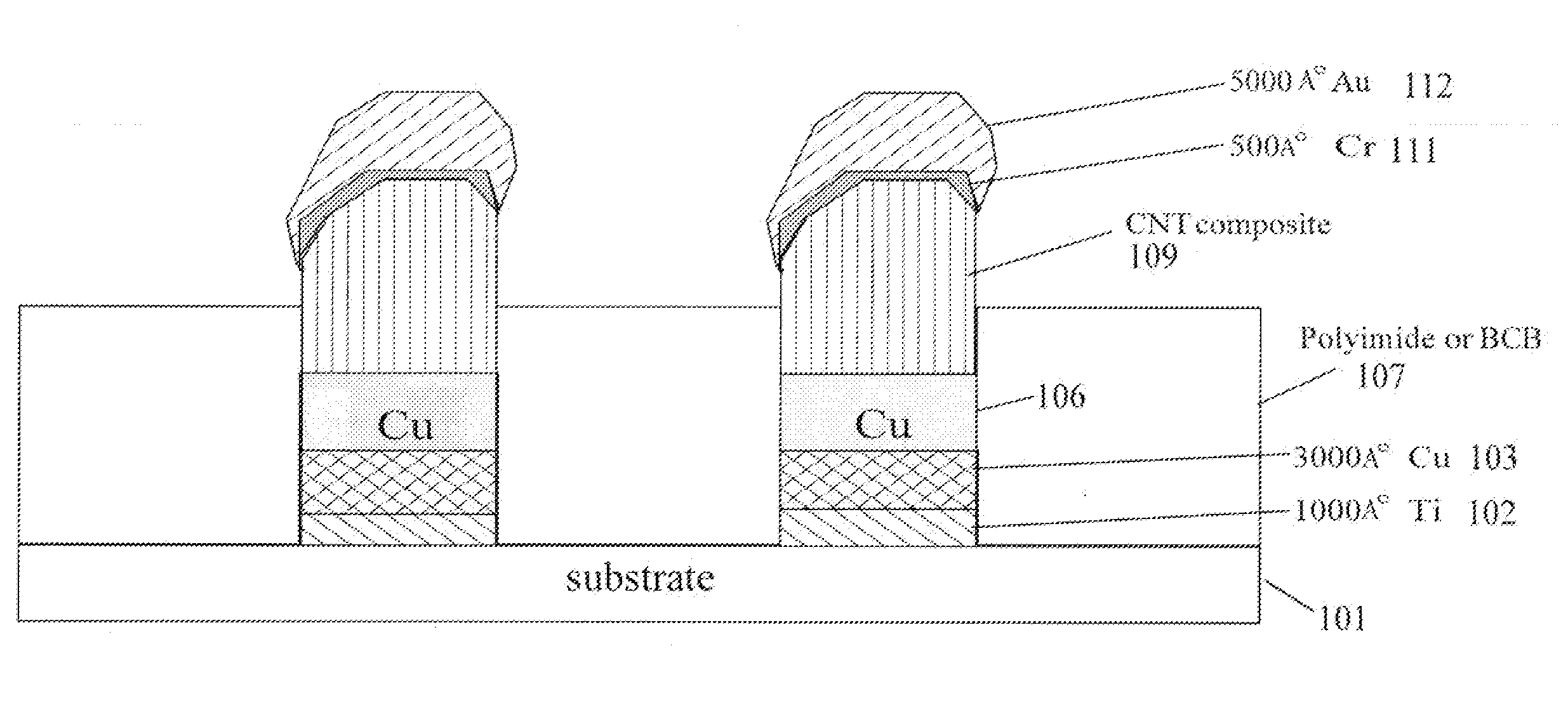
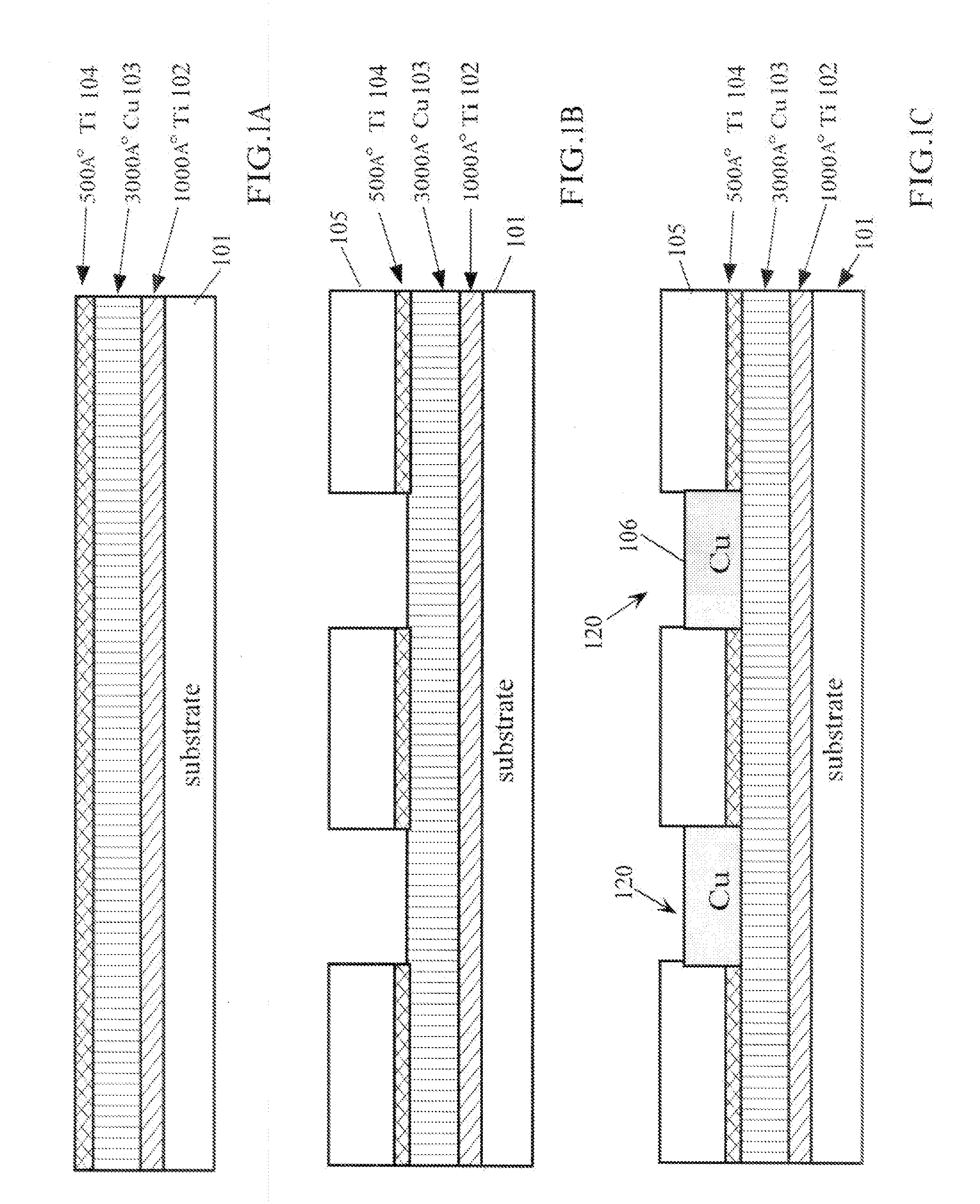
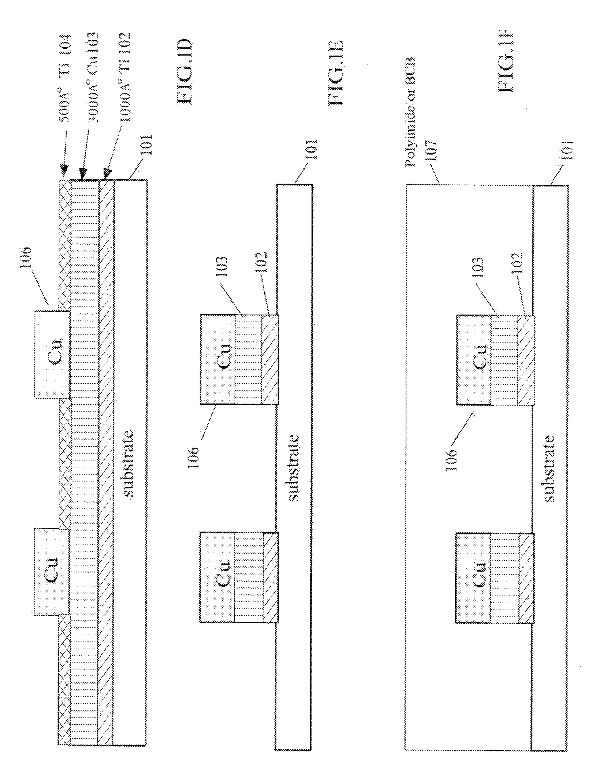
[0006]U.S. Pat. No. 5,508,228, hereby incorporated by reference, describes electrically connective complaint bumps for an adhesive flip chip integrated circuit device and methods for making the same. The compliant bumps are advantageous over traditional flip chip connectors, such as solid metal bumps, that can lose electrical contact between two integrated circuits for a variety of reasons, such as gross delamination and tensile stress cracking. Furthermore, solid metal bumps suffer from adhesive creep-relaxation. In addition, the coefficient of thermal expansion of a solid metal bump is typically much lower than that of the adhesive that holds the flip chip device in contact with the substrate. As the flip chip increases in temperature, therefore, the adhesive expands faster than does the bump. This causes the flip chip to separate from the substrate. This thermal expansion, consequently, opens the circuit between the flip chip and substrate and electrical conductivity is sacrifice...


PUM


Abstract

Complaint bumps used for interconnections between integrated circuit chips are made with carbon nanotubes.

Description

[0001]This application for patent claims priority to U.S. Provisional Patent Application Ser. No. 60 / 808,800, which is hereby incorporated by reference herein.BACKGROUND INFORMATION[0002]High-frequency, high-power (e.g., amplifiers) present a host of problems for circuit designers. For example, amplifier integrated circuits were traditionally mounted to other integrated circuit using a “face up” methodolody. In other words, the amplifier integrated circuit was coupled, face up, to the other integrated circuit. The amplifier communicated with the other integrated circuit via connecting wires. This orientation allowed heat generated from the amplifier to dissipate. However, as high-power amplifiers began to function at increasingly higher frequencies, the use of such connecting wired proved problematic. For instance, the connecting wires generated high inductances that lowered the amplification capabilities of the amplifier. To counter the high inductances, the amplifiers were coupled...

Claims


Application Information

Patent Timeline
Patent Type & Authority Applications(United States)
IPC IPC(8): H01L23/48
CPCH01L24/11H01L2224/1147H01L2924/01033H01L2924/01024H01L2924/01019H01L2924/01006H01L2924/00013H01L24/13H01L2924/3511H01L2224/1308H01L2224/13083H01L2224/13144H01L2224/13147H01L2224/13171H01L2924/01022H01L2924/01029H01L2924/01074H01L2924/01079H01L2924/01082H01L2924/14H01L2924/30107H01L2924/00014H01L2224/13099H01L24/03H01L24/05H01L2224/05001H01L2224/05026H01L2224/0508H01L2224/05147H01L2224/05166H01L2224/0557H01L2224/05571H01L2224/05647
Inventor YANIV, ZVI
Owner APPLIED NANOTECH HLDG
Why Eureka
Try Eureka