Electrically inactive via for electromigration reliability improvement

a via and inactive technology, applied in the direction of semiconductor devices, semiconductor/solid-state device details, electrical apparatus, etc., can solve the problems of metallization layer problems, void regions within copper vias can be formed, problems such as electromigration, etc., to facilitate semiconductor device fabrication and operation, mitigate void creation and/or void migration, and reduce tensile stress

Active Publication Date: 2008-01-24
TEXAS INSTR INC
View PDF14 Cites 11 Cited by
  • Summary
  • Abstract
  • Description
  • Claims
  • Application Information

AI Technical Summary

Benefits of technology

[0006]Aspects of the present invention facilitate semiconductor device fabrication and operation by employing isolated conductive regions to mitigate void creation and / or void migration due to electromigration. The aspects can be employed with single-damascene and / or dual-damascene processes. One or more electrically isolated conductive regions, such as isolated vias, are positioned and in contact with a conductive layer such as a metal line between cathode and anode portions. The isolated conductive regions create flux divergence positions that mitigate tensile stress created at the cathode portion and elsewhere. As a result, the tensile stress does not exceed a critical or threshold value and mitigates void formation or nucleation.

Problems solved by technology

As device sizes continue to shrink to enable fast operational speeds and higher densities, problems can be encountered for metallization layers.
As a result, problems such as electromigration can occur.
In, for example, copper vias, electromigration can cause copper ions to migrate and result in formation of void regions within the copper vias.

Method used


Image

  • Electrically inactive via for electromigration reliability improvement
  • Electrically inactive via for electromigration reliability improvement
  • Electrically inactive via for electromigration reliability improvement

Examples


Embodiment Construction

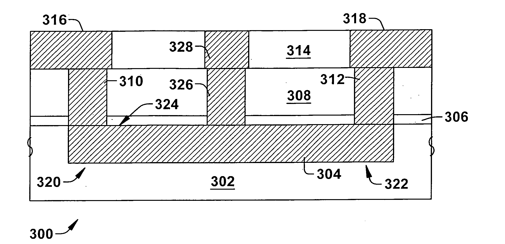
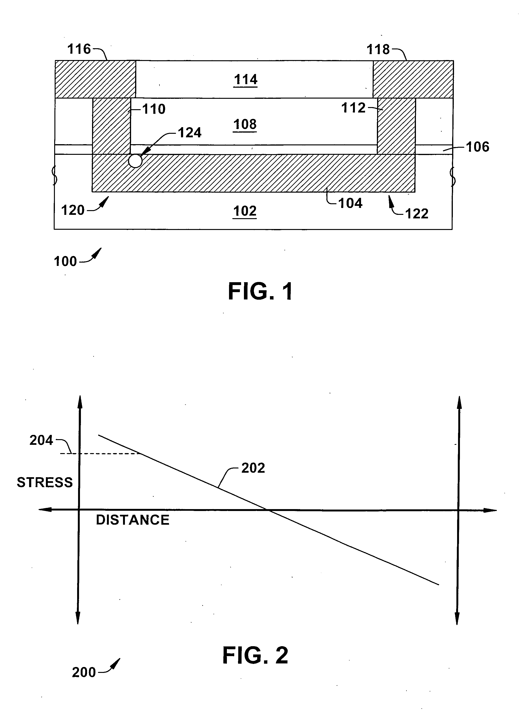
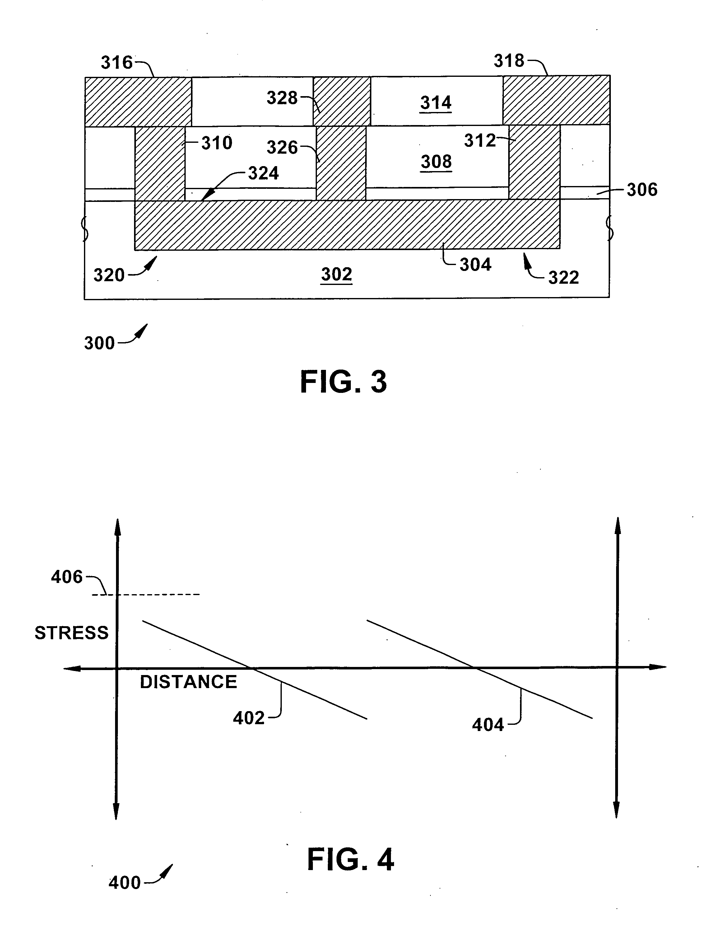
[0017]The present invention will now be described with respect to the accompanying drawings in which like numbered elements represent like parts. The figures provided herewith and the accompanying description of the figures are merely provided for illustrative purposes. One of ordinary skill in the art should realize, based on the instant description, other implementations and methods for fabricating the devices and structures illustrated in the figures and in the following description.

[0018]Aspects of the present invention facilitate semiconductor device fabrication and operation by employing isolated conductive regions to mitigate void creation and / or void migration due to electromigration. The aspects can be employed with single-damascene and / or dual-damascene processes. One or more electrically isolated conductive regions, such as isolated vias, are positioned and in contact with a conductive layer such as a metal line between cathode and anode portions. The isolated conductive ...


PUM


Abstract

A semiconductor device 300 includes a metal line 304 formed in a first dielectric layer 302. A capping layer 306 is formed the metal line 304. A second dielectric layer 308 is formed over the first dielectric layer 302 and the metal line 304. A first via 310 is formed in the second dielectric layer 308 and in contact with the metal line 304. A second via 312 is formed in the second dielectric layer 308 and in contact with the metal line 304, and is positioned a distance away from the first via 310. An electrically isolated via 326 is formed in the second dielectric layer 308 and in contact with the metal line 304 and in between the first via 310 and the second via 312. A third dielectric layer 314 is formed over the second dielectric layer 308. First and second trenches 316, 318 are formed in the third dielectric layer 314 and in contact with the first via 310 and the second via 312, respectively. An isolated trench 328 is formed in the third dielectric layer and in contact with the isolated via 326. The isolated via 326 mitigates void formation and / or void migration during operation / conduction with electrons traveling from the first trench 316 to the second trench 318 via the metal line 304.

Description

FIELD OF THE INVENTION[0001]The present invention relates generally to semiconductor fabrication and, more particularly, to devices and methods that mitigate electromigration induced failure by employing an inactive punch-via.BACKGROUND OF THE INVENTION[0002]Integrated circuits and semiconductor devices are fabricated by performing a number of fabrication processes that form various components and regions, such as source / drain regions, gate structures, isolation regions, and the like. One set of structures formed and / or present in semiconductor devices are metallization layers, which provide electrical connections between various components within the devices and external connections.[0003]The metallization layers typically comprise trenches and vias formed in single or dual damascene fabrication processes. The trenches and vias are comprised of conductive materials and are separated by insulating layers comprised of dielectric material to, for example, mitigate crosstalk between va...

Claims


Application Information

Patent Timeline
Patent Type & Authority Applications(United States)
IPC IPC(8): H01L23/52H01L21/4763
CPCH01L23/522H01L23/53295H01L23/5226H01L2924/0002H01L2924/00
Inventor LEE, KI-DONPARK, YOUNG-JOONOGAWA, ENNIS TAKASHI
Owner TEXAS INSTR INC
Why Eureka
Try Eureka