Electrical and thermal contact for use in semiconductor devices

a technology of electrical and thermal contact, which is applied in the direction of semiconductor devices, semiconductor/solid-state device details, electrical apparatus, etc., can solve the problems of increasing potential, affecting the fabrication of electrical and thermal contacts, and affecting the appearance of electrical contacts, etc., to achieve the effect of facilitating the fabrication of relatively small electrical and thermal contacts

Inactive Publication Date: 2007-02-06
ROUND ROCK RES LLC
View PDF21 Cites 0 Cited by
  • Summary
  • Abstract
  • Description
  • Claims
  • Application Information

AI Technical Summary

Benefits of technology

[0013]Fabricating the electrical and thermal contact includes forming a dielectric layer around the lateral peripheral portions of a semiconductor device structure to be contacted, patterning the dielectric layer to expose at least a portion of the semiconductor device structure to be contacted, such as an active device region thereof, depositing a first thin conductive layer, depositing another dielectric layer adjacent the first thin conductive layer, patterning the dielectric layer to define a thermal insulator component, depositing a second thin conductive layer adjacent the thermal insulator component and in electrical communication with the first thin conductive layer, and patterning the first and second thin conductive layers to define the intermediate conductive layer and the contact layer, respectively. The dielectric layer is fabricated from an electrically and thermally conductive material. Preferably, during patterning of the dielectric layer, the first thin conductive layer is utilized as an etch stop. The processes that may be employed to fabricate the electrical and thermal contact facilitate the fabrication of a relatively small electrical and thermal contact when compared with conventional metal contacts.

Problems solved by technology

Nevertheless, the application of too great a current to memory elements, such as fuse and antifuse elements, increases the potential that various other components of the EEPROM of which they are a part, including without limitation the gate oxide layer, transistors, and other structures on the surface thereof, may be damaged.
As noted previously, programming pulses which comprise high electrical voltages may damage various components of an EEPROM, including, without limitation, the gate oxide layer, transistors and other structures on the surface of the EEPROM.
Further, due to the high rate at which many conventional metal contacts dissipate heat, such contacts may necessitate the input of even greater amounts of current in order to adequately heat and activate an antifuse element.
Moreover, the typical use of conventional, relatively large metal contacts on such EEPROMs is somewhat undesirable from the standpoint that such contacts consume a great deal of surface area or “real estate” on the surface of the semiconductor device.
Thus, conventional metal contacts limit the density of active device regions on the semiconductor device.
The dissipation of heat away from the memory cell through the metal contact is especially undesirable when the memory cell includes a phase change component, such as a chalcogenide material layer, such as the EEPROM devices disclosed in U.S. Pat. No. 5,789,758 (hereinafter “the '758 patent”), which issued to Alan R. Reinberg on Aug. 4, 1998.

Method used


Image

  • Electrical and thermal contact for use in semiconductor devices
  • Electrical and thermal contact for use in semiconductor devices
  • Electrical and thermal contact for use in semiconductor devices

Examples


Embodiment Construction

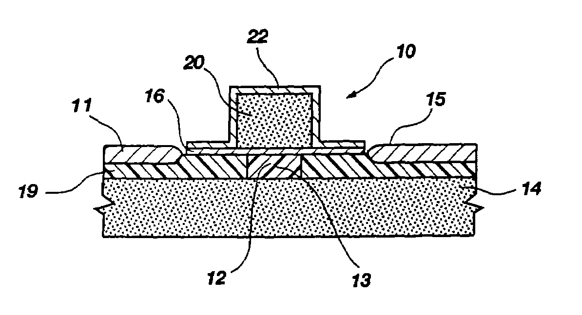
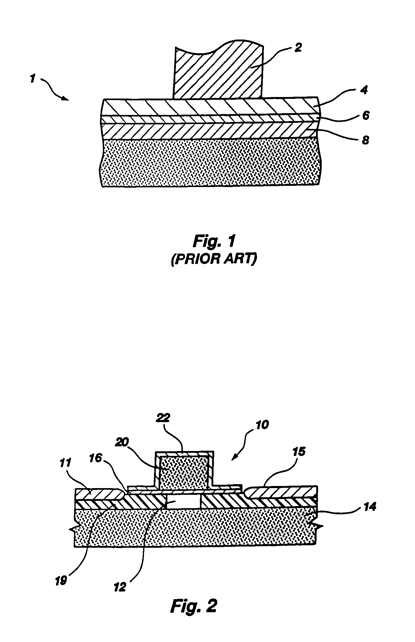
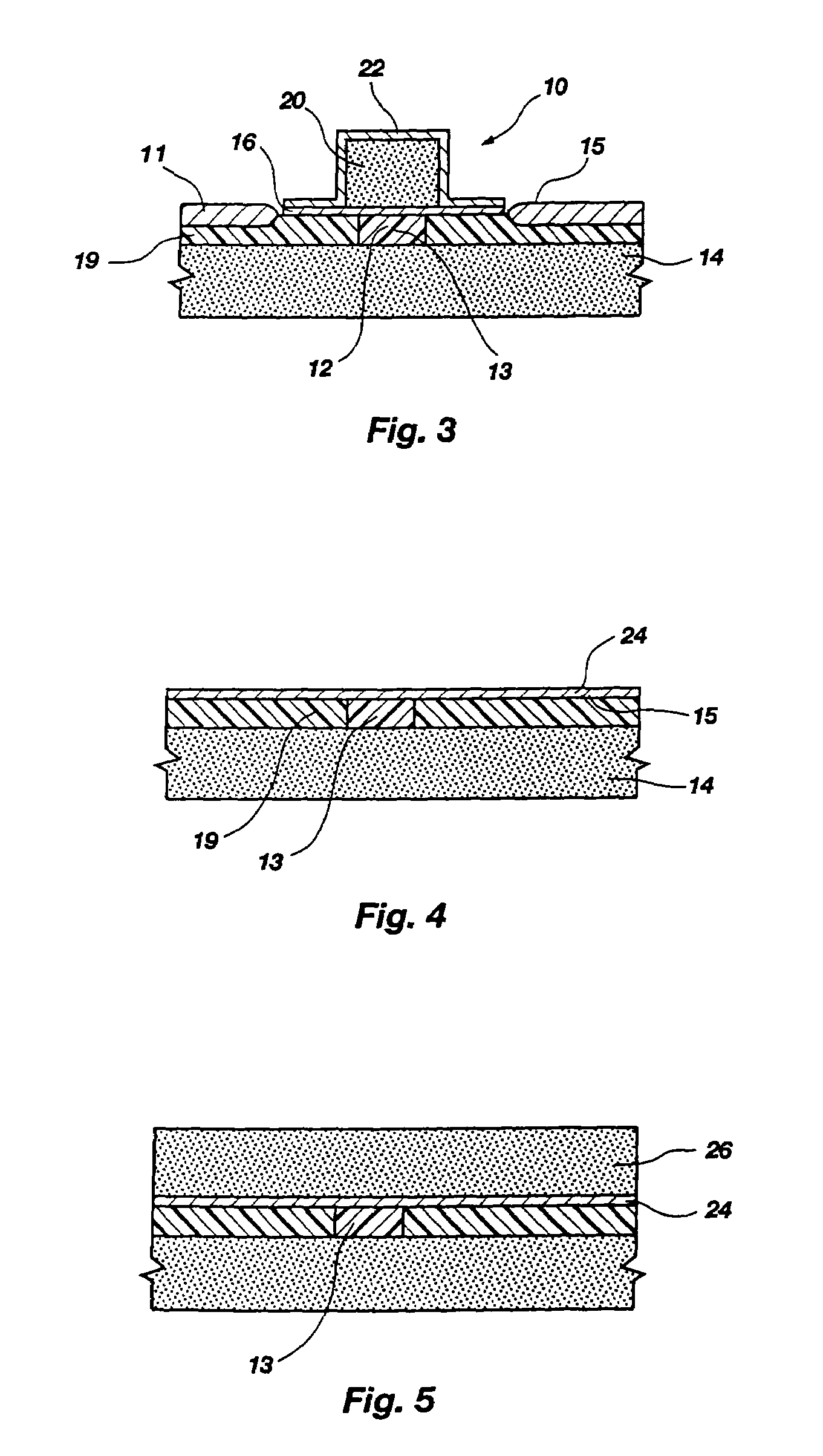
[0025]The present invention comprises an electrical and thermal contact for a contacted structure of a semiconductor device. With reference to FIGS. 2 and 3, in a preferred embodiment, the electrical and thermal contact 10 is disposed on a surface 15 of a semiconductor device 14. Electrical and thermal contact 10 may be positioned adjacent a contacted structure 12, such as an antifuse or other memory element, that is exposed through oxide layer 11, such that it electrically and thermally contacts the contacted structure 12. Preferably, electrical and thermal contact 10 contacts an electrically conductive phase change component 13 of contacted structure 12 (FIG. 3), such as the memory element disclosed in the '758 patent. Preferably, contacted structure 12 includes a dielectric element 19 surrounding the lateral peripheral portions of phase change component 13 to thermally and electrically insulate the latter.

[0026]Electrical and thermal contact 10 includes a thin, intermediate condu...


PUM


Abstract

An electrical and thermal contact for use in a semiconductor device. The electrical and thermal contact includes an intermediate conductive layer, an insulator component, and a contact layer. The intermediate conductive layer may contact a structure of the semiconductor device. The insulator component, which is fabricated from a thermally and electrically insulative material, may be sandwiched between the intermediate conductive layer and the contact layer, which may substantially envelop the insulator component. The electrical and thermal contact may be fabricated by a process which includes forming a first thin layer on a surface of the semiconductor device, depositing a dielectric layer adjacent the first thin layer, patterning the dielectric layer to define the insulator component, forming a second thin layer adjacent the insulator component and in partial contact with the first thin layer, and patterning the first and second thin layers to define the intermediate conductive layer and the contact layer, respectively. Due to its structure, which requires relatively little electrical current to generate a desired amount of heat, the electrical and thermal contact effectively contains heat within and prevents heat from dissipating from a contacted structure, and is particularly useful for contacting and inducing a change in the electrical conductivity of structures which include phase change materials.

Description

BACKGROUND OF THE INVENTION[0001]1. Field of the Invention[0002]The present invention relates to an electrical and thermal contact for use in semiconductor devices. Particularly, the present invention relates to an electrical and thermal contact which reduces the amount of energy input that is required in order to switch a semiconductor device structure that is contacted thereto between two or more states. More specifically, the electrical and thermal contact of the present invention includes thin conductive layers which envelop an insulator component. The electrical and thermal contact is particularly useful for switching contacted structures that include a phase change component between two or more states of electrical conductivity.[0003]2. Background of Related Art[0004]Electrically erasable programmable memory devices (EEPROMS) typically include several memory elements that may be switched between a first logic state and a second logic state. A first logic state may be an inacti...

Claims


Application Information

Patent Timeline
Patent Type & Authority Patents(United States)
IPC IPC(8): H01L29/00H01L23/525H01L45/00
CPCH01L45/06H01L45/1233H01L45/141H01L45/16H01L45/128H01L23/5252Y10S438/90H01L2924/0002H10N70/231H10N70/861H10N70/882H10N70/826H10N70/011H01L2924/00
Inventor REINBERG, ALAN R.
Owner ROUND ROCK RES LLC
Why Eureka
Try Eureka