Method for conditioning a polishing pad

a polishing pad and polishing technology, applied in the field of integrated circuit fabrication, can solve the problems of increasing the production cost per substrate, increasing reducing the processing cost per substrate, so as to increase the removal rate and increase the removal rate of conductive materials

Inactive Publication Date: 2008-01-24
APPLIED MATERIALS INC
View PDF8 Cites 4 Cited by
  • Summary
  • Abstract
  • Description
  • Claims
  • Application Information

AI Technical Summary

Benefits of technology

[0012] The present invention provides a method of conditioning processing pads that increases the removal rate. According to embodiments of the present invention, conductive material removal rates will be increased during the ECMP process if the direction of rotation of the processing pad relative to the conditioning disc is opposite the direction of rotation of the processing pad relative to the substrate.

Problems solved by technology

Lower removal rate results in a longer processing time, thereby increasing the production cost per substrate.
Because the reconditioning process is generally time-consuming, a longer period between such reconditioning significantly reduces ECMP system downtime, which also lowers processing cost per substrate.

Method used


Image

  • Method for conditioning a polishing pad
  • Method for conditioning a polishing pad
  • Method for conditioning a polishing pad

Examples


Embodiment Construction

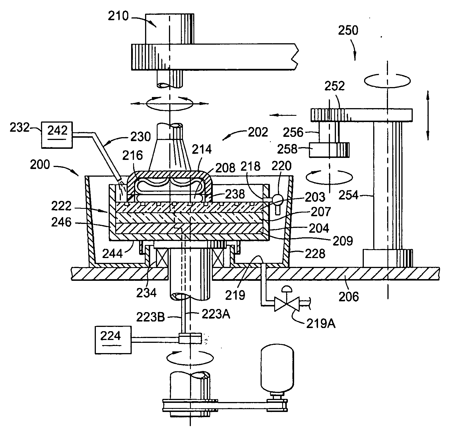
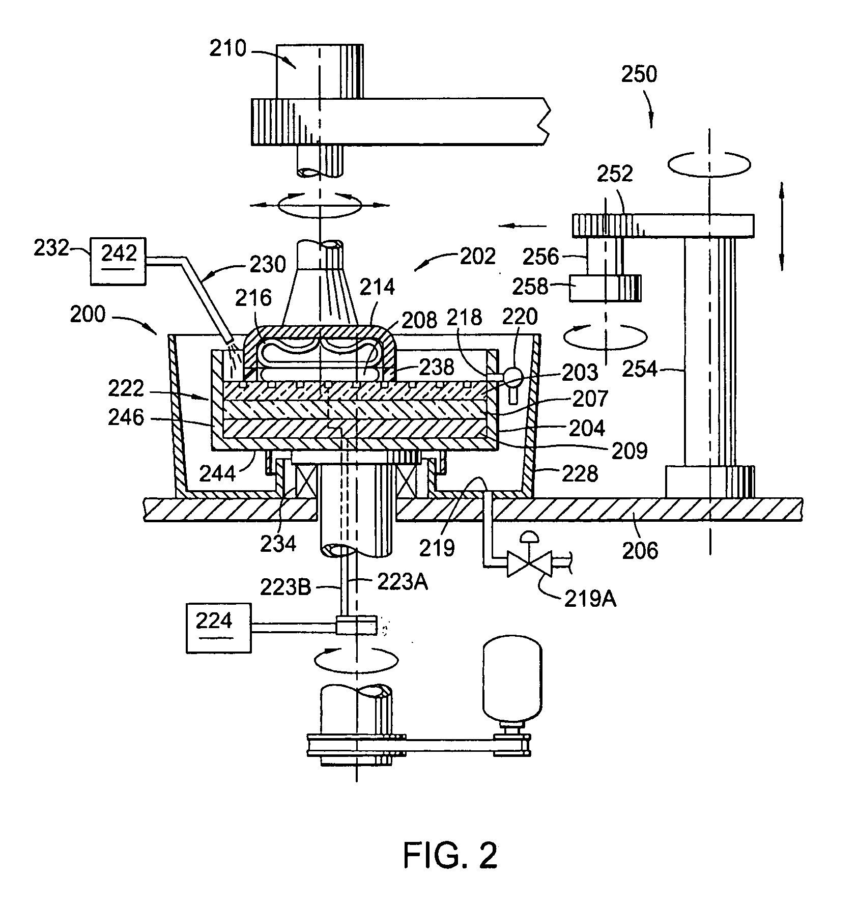
[0026]FIG. 2 is a cross-sectional view of one example of an ECMP station 200 that may be used to practice aspects of the invention. The process cell 200 generally includes a basin 204 and a polishing head 202. A substrate 208 is retained in the polishing head 202 and lowered into the basin 204 during processing in a face-down, i.e., production side down, orientation. An electrolyte, as described herein, flows into the basin 204 and is in contact with the surface of substrate 208 and a processing pad assembly 222, while the polishing head 202 places the substrate 208 in contact with the processing pad assembly 222. The basin 204 includes the processing pad assembly 222, a bottom 244 and sidewalls 246 that define a container that houses the processing pad assembly 222. The sidewalls 246 include a port 218, formed therethrough to allow removal of polishing composition from the basin 204. The port 218 is coupled to a valve 220 to selectively drain or retain the polishing composition in ...


PUM

PropertyMeasurementUnit
voltageaaaaaaaaaa
radial velocityaaaaaaaaaa
velocityaaaaaaaaaa

Abstract

A method of conditioning processing pads increases the removal rate of conductive material from a substrate surface during polishing. In this method, the direction of rotation of the processing pad relative to the conditioning disc during conditioning is opposite the direction of rotation of the processing pad relative to the substrate during polishing.

Description

BACKGROUND OF THE INVENTION [0001] 1. Field of the Invention [0002] Embodiments of the present invention generally relate to the fabrication of integrated circuits and more particularly to the removal of conductive material from a substrate. [0003] 2. Description of the Related Art [0004] In VLSI and ULSI semiconductor manufacturing, reliable formation of multilevel interconnects is important to the continued effort to increase circuit density and quality of individual substrates and die. Multilevel interconnects are formed using sequential material deposition and material removal techniques on a substrate surface to form features therein. As layers of materials are sequentially deposited and removed, the uppermost surface of the substrate may become non-planar across its surface and require planarization prior to further processing. Planarization, or “polishing,” is a process in which material is removed from the surface of the substrate to form a generally even, planar surface. Pl...

Claims


Application Information

Patent Timeline
Patent Type & Authority Applications(United States)
IPC IPC(8): B24B1/00
CPCB24B53/017
Inventor JIA, RENHEDIAO, JIEWANG, YOUTSAI, STAN D.ATKINSON, JIM K.KARUPPIAH, LAKSHMANANCHEN, LIANG-YUH
Owner APPLIED MATERIALS INC
Why Eureka
Try Eureka