Method and system for testing semiconductor memory device using internal clock signal of semiconductor memory device as data strobe signal

Active Publication Date: 2008-01-31
SAMSUNG ELECTRONICS CO LTD
View PDF15 Cites 5 Cited by
  • Summary
  • Abstract
  • Description
  • Claims
  • Application Information

AI Technical Summary

Benefits of technology

[0008]An embodiment of the present invention provides a test method capable of increasing the number of semiconductor memory modules that can be simultaneously tested so as to reduce a test time for a unit memory module.
[0009]An embodiment of the present invention also provides a semiconductor memory device capable of increasing the number of semiconductor memory modules that can be simultaneously tested so as to reduce a test time for a unit memory module.

Problems solved by technology

However, the number of semiconductor memory modules that can be simultaneously tested is restricted by the number of test channels of a test device, and the number of test channels is restricted by the number of signals applied to the semiconductor memory modules.

Method used


Image

  • Method and system for testing semiconductor memory device using internal clock signal of semiconductor memory device as data strobe signal
  • Method and system for testing semiconductor memory device using internal clock signal of semiconductor memory device as data strobe signal
  • Method and system for testing semiconductor memory device using internal clock signal of semiconductor memory device as data strobe signal

Examples


Embodiment Construction

[0019]The present invention will now be described more fully with reference to the accompanying drawings, in which exemplary embodiments of the invention are shown. The invention may, however, be embodied in many different forms and should not be construed as being limited to the embodiments set forth herein; rather, these embodiments are provided so that this disclosure will be thorough and complete, and will fully convey the concept of the invention to those of ordinary skill in the art. Throughout the drawings, like reference numerals refer to like elements.

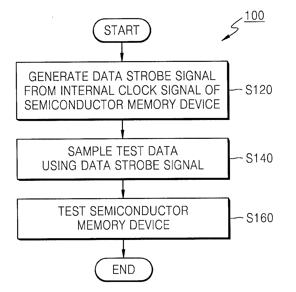
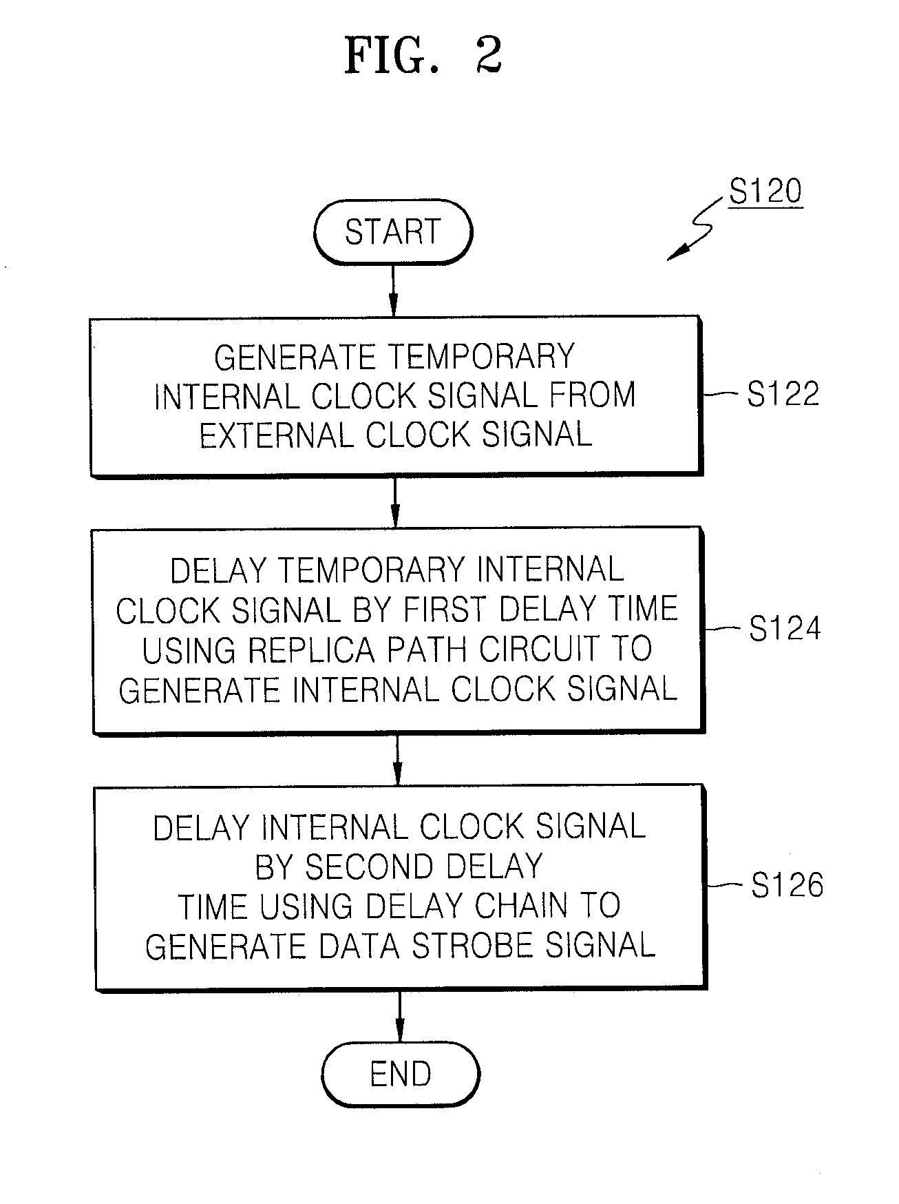
[0020]FIG. 1 is a flow chart of a method 100 of testing a semiconductor memory device according to an embodiment of the present invention. Referring to FIG. 1, the method 100 of testing a semiconductor memory device according to an embodiment of the present invention includes an operation S120 of generating a data strobe signal using an internal clock signal of the semiconductor memory device, an operation S140 of sampling tes...


PUM


Abstract

Provided are a method and system for testing a semiconductor memory device using an internal clock signal of the semiconductor memory device as a data strobe signal. The internally-generated data strobe signal may be delayed to synchronize with test data. Because a test device need not supply the data strobe signal, the number of semiconductor memory modules that can be simultaneously tested can be increased, and an average test time for a unit memory module can be decreased.

Description

BACKGROUND OF THE INVENTION[0001]1. Field of the Invention[0002]The present invention relates generally to a semiconductor memory device, and more particularly, but not by way of limitation, to a method and system for testing a semiconductor memory device at high speed using a data storage signal generated from an internal clock signal of the semiconductor memory device so as to increase the number of memory modules that can be simultaneously tested and reduce a test time for a unit memory module.[0003]This application claims the benefit of Korean Patent Application No. 10-2006-0072248, filed on Jul. 31, 2006, in the Korean Intellectual Property Office, the disclosure of which is incorporated herein in its entirety by reference.[0004]2. Description of the Related Art[0005]As semiconductor memory devices become highly integrated, the time required to test the semiconductor memory devices is increased. Accordingly, high-speed test techniques have been developed in order to reduce the ...

Claims


Application Information

Patent Timeline
IPC IPC(8): G11C29/00G11C7/00
CPCG11C5/04G11C29/14G11C29/12015G11C29/00
Inventor KIM, JUN-BAERYU, JIN-HOPARK, SUNG-MAN
Owner SAMSUNG ELECTRONICS CO LTD
Why Eureka
Try Eureka