Process for manufacture of ceramic capacitors using ink jet printing

a ceramic capacitor and ink jet printing technology, applied in the direction of fixed capacitors, stacked capacitors, fixed capacitor details, etc., can solve the problems of increasing manufacturing difficulties, increasing the difficulty of manufacturing devices with minimal layer distortion, and affecting the physical properties of layer distortion

Inactive Publication Date: 2008-01-31
KEMET ELECTRONICS CORP
View PDF0 Cites 22 Cited by
  • Summary
  • Abstract
  • Description
  • Claims
  • Application Information

AI Technical Summary

Benefits of technology

[0006]It is an object of the invention to provide a method for manufacturin...

Problems solved by technology

As with any electronic component the ongoing desire for miniaturization places continued burdens on every aspect of product properties and product manufacture thereby forcing those of skill in the art to continue to advance the art.
As layer counts in a multilayer device increase and as the dielectric and electrode thicknesses decrease the manufacturing difficulties increase.
In particular, it becomes increasingly more difficul...

Method used


Image

  • Process for manufacture of ceramic capacitors using ink jet printing
  • Process for manufacture of ceramic capacitors using ink jet printing
  • Process for manufacture of ceramic capacitors using ink jet printing

Examples


Embodiment Construction

[0029]The instant invention will be described with reference to the various drawings forming an integral part of the specification. In the various drawings similar elements will be numbered accordingly.

[0030]An improved method for manufacturing a multilayer ceramic device is provided herein. The method includes applying consecutive layers of electrode and dielectric layers by ink jet printing techniques without reliance on transfer sheets for the layers.

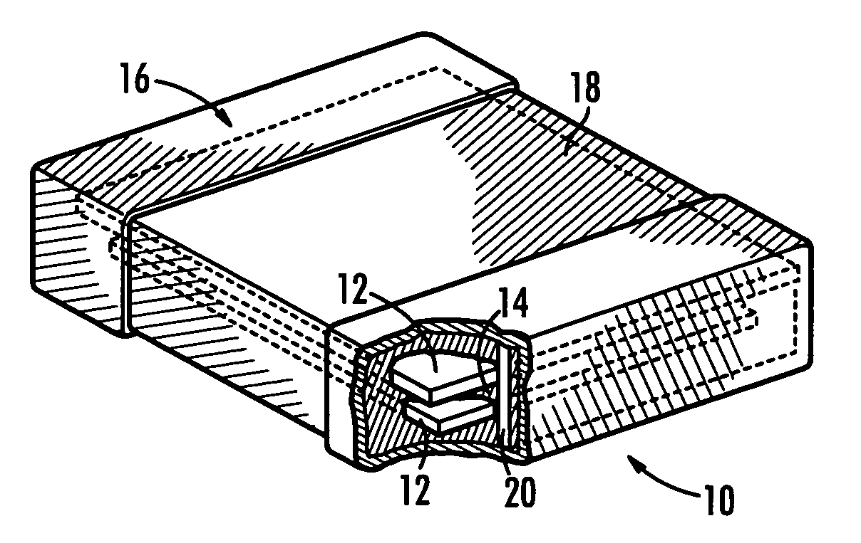
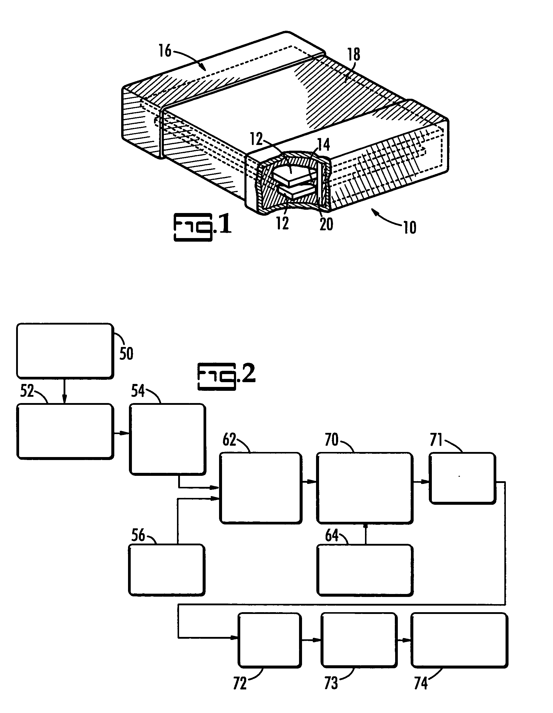
[0031]A multilayer ceramic device is illustrated in FIG. 1. In FIG. 1, the device, generally represented at 10, comprises internal electrodes, 12, with dielectric, 14, there between. As would be realized the plates are alternately in contact with external electrodes, 16, of opposite polarity. External electrodes are also referred to as terminations. A ceramic dielectric, 18, acts as a protective barrier. An internal layer, 20, facilitates electrical connectivity between the internal electrode and the external electrodes. Two plates a...


PUM

PropertyMeasurementUnit
Electrical conductoraaaaaaaaaa

Abstract

A process for forming a multilayer ceramic device. The device includes forming a ceramic precursor layer followed by ink jet printing in alternating order an electrode precursor in a predetermined pattern on the ceramic precursor layer to form an electrode and a ceramic ink on the electrode. The ceramic precursor is then sintered.

Description

BACKGROUND OF THE INVENTION[0001]The present invention is related to an improved method for forming a multilayer device and a device formed thereby. More particularly, the present invention is related to the formation of a multilayer device by ink jet printing consecutive layers to form a multilayered device.[0002]Manufacturing of multilayer devices by lamination is a standard practice particularly in the manufacture of multi-layer ceramic capacitors (MLCC). As with any electronic component the ongoing desire for miniaturization places continued burdens on every aspect of product properties and product manufacture thereby forcing those of skill in the art to continue to advance the art. It is highly desirable to increase the layer count while concurrently decreasing the layer thickness.[0003]As layer counts in a multilayer device increase and as the dielectric and electrode thicknesses decrease the manufacturing difficulties increase. In particular, it becomes increasingly more diff...

Claims


Application Information

Patent Timeline
IPC IPC(8): B05D5/12C03B29/00H01G4/06
CPCC04B35/4682H01G13/006C04B2235/3208C04B2235/3213C04B2235/3224C04B2235/3225C04B2235/3244C04B2235/3262C04B2235/36C04B2235/6562C04B2235/6565C04B2235/6567C04B2235/6582C04B2235/6584C04B2235/6588C04B2235/663H01G4/0085H01G4/2325H01G4/30C04B2235/3206
Inventor SKAMSER, DANIEL J.RANDALL, MICHAEL S.HOCHHEIMER, J. THOMASTAJUDDIN, AZIZUDDIN
Owner KEMET ELECTRONICS CORP
Why Eureka
Try Eureka