Methods of controlling morphology during epitaxial layer formation

a technology of epitaxial layer and morphology, which is applied in the direction of polycrystalline material growth, crystal growth process, chemically reactive gas, etc., can solve the problems of limited, or no, deposition of epitaxy material, and difficult production of ultra shallow source/drain junction. achieve the effect of smooth surface morphology and fast deposition ra

Active Publication Date: 2008-01-31
APPLIED MATERIALS INC
View PDF97 Cites 29 Cited by
  • Summary
  • Abstract
  • Description
  • Claims
  • Application Information

AI Technical Summary

Problems solved by technology

As smaller transistors are manufactured, ultra shallow source / drain junctions are becoming more challenging to produce.
Therefore, by changing the concentration of an etchant gas, the net selective process results in deposition of epitaxy material and limited, or no, deposition of polycrystalline material.
On the other hand, the ultra shallow source / drain junction inevitably results in increased series resistance.
Also, junction consumption during silicide formation increases the series resistance even further.
However, current selective epitaxy processes have some drawbacks.
Also, harmful over etching of substrate features may occur.
Such high temperatures are not desirable during a fabrication process due to thermal budget considerations and possible uncontrolled nitridation reactions to the substrate surface.

Method used


Image

  • Methods of controlling morphology during epitaxial layer formation
  • Methods of controlling morphology during epitaxial layer formation
  • Methods of controlling morphology during epitaxial layer formation

Examples


Embodiment Construction

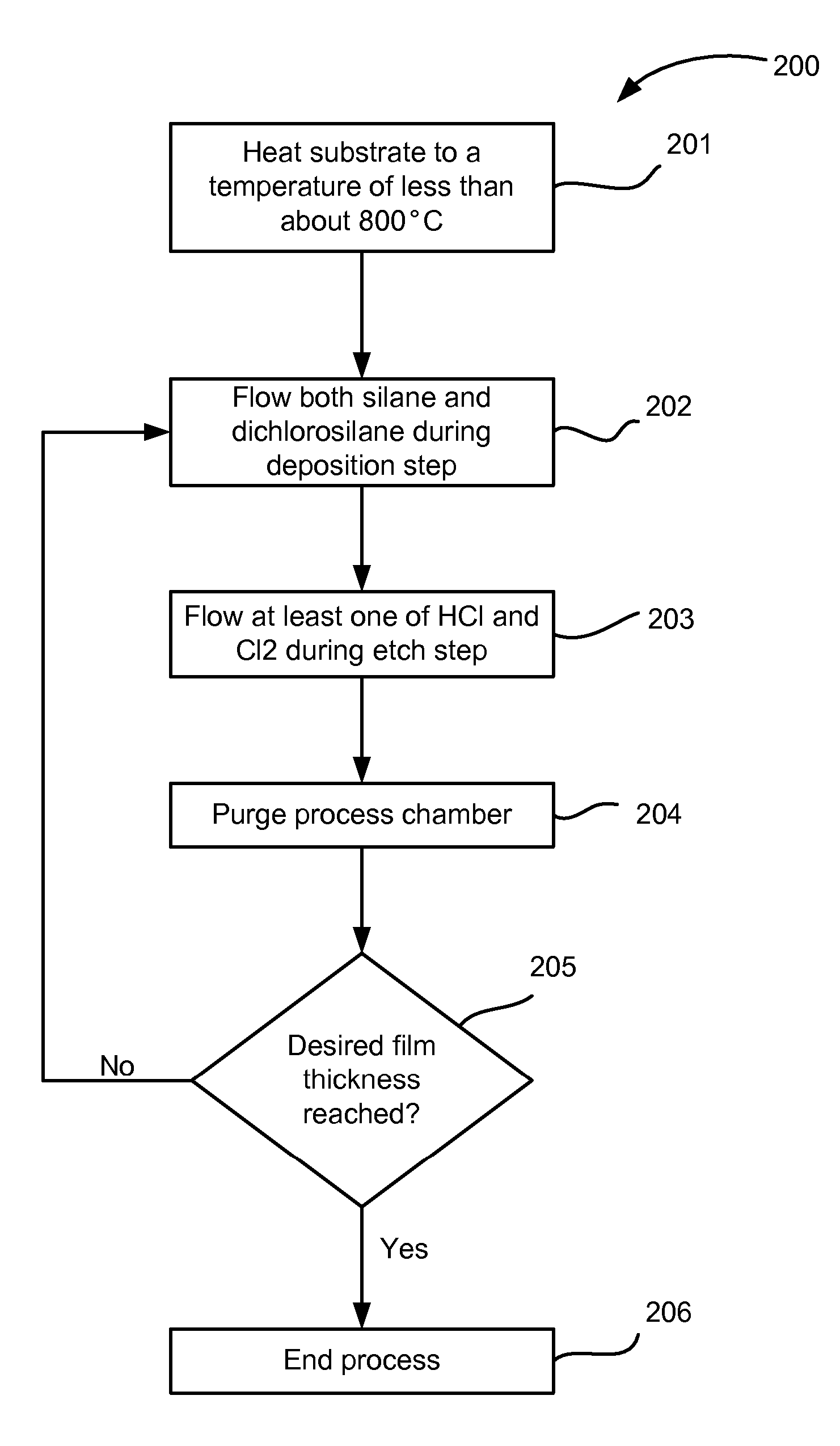
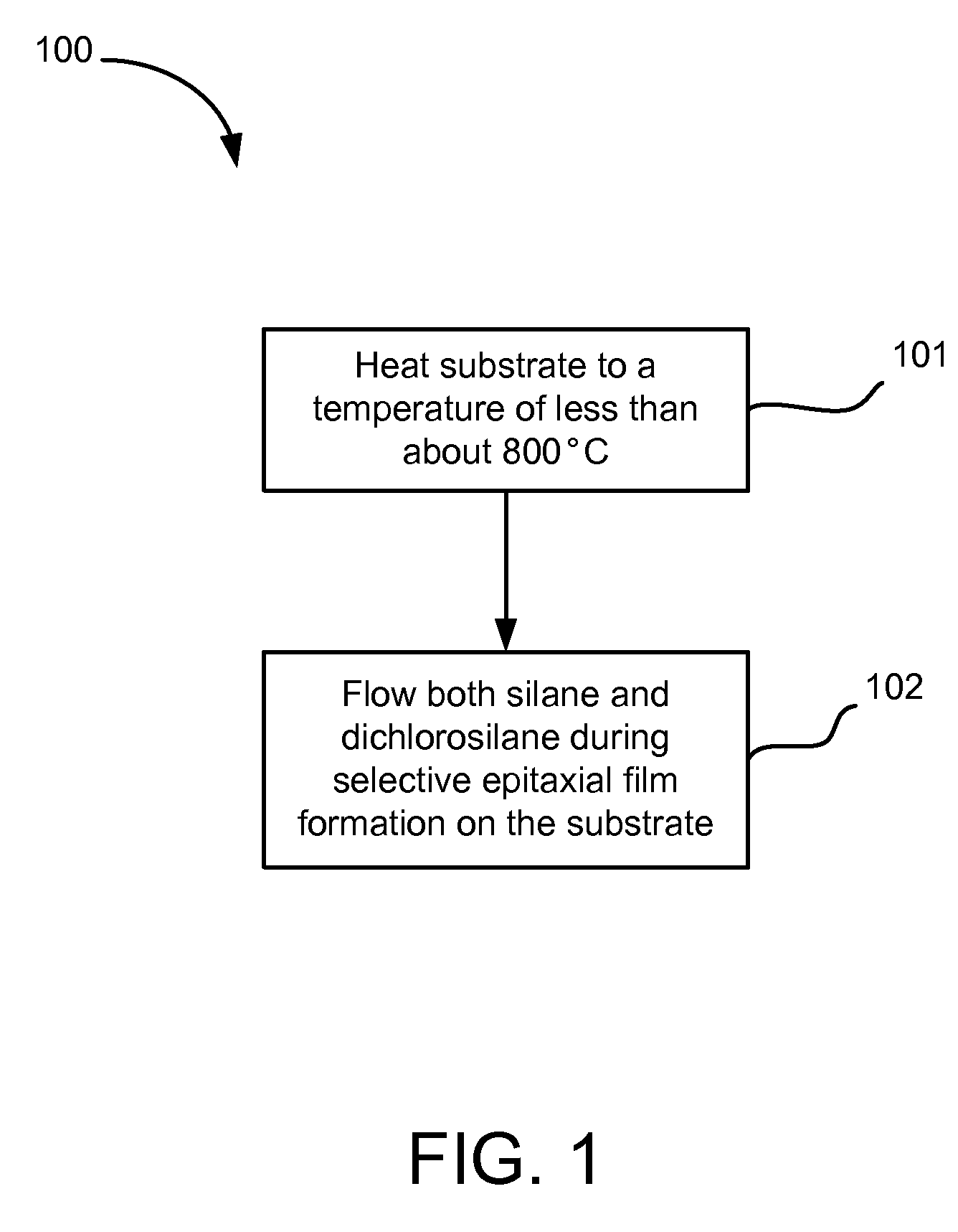
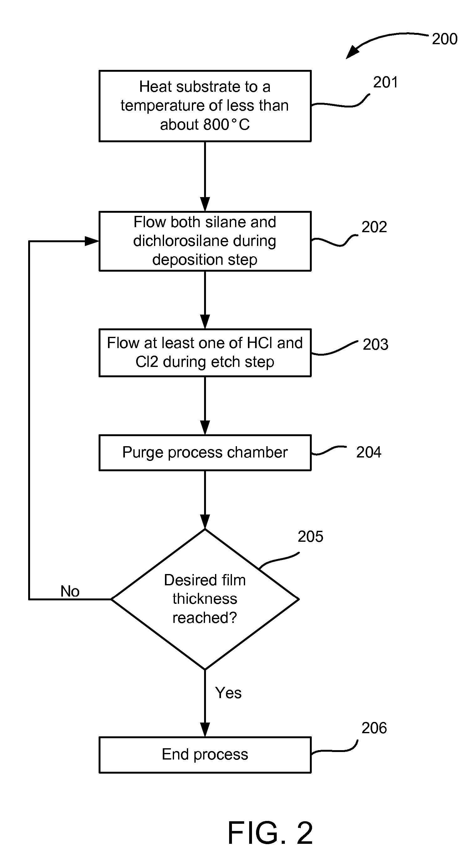
[0017] During a selective epitaxial growth process on a silicon substrate patterned with dielectric films, formation of single-crystal semiconductor occurs only on the exposed silicon surfaces (e.g., not on the dielectric surfaces). Selective thickness is defined as the maximum film thickness obtained on the silicon surfaces prior to the onset of film growth or nucleation on the dielectric surfaces.

[0018] Selective epitaxial growth processes may include simultaneous etch-deposition processes as well as alternating gas supply processes. In a simultaneous etch-deposition process, both etchant species and deposition species are flowed simultaneously. As such, an epitaxial layer is simultaneously deposited and etched during its formation.

[0019] U.S. patent application Ser. No. 11 / 001,774, filed Dec. 1, 2004 (Docket No. 9618), describes an alternating gas supply (AGS) process for forming epitaxial layers on a substrate. During an AGS process, an epitaxial deposition process is conducte...


PUM

PropertyMeasurementUnit
temperatureaaaaaaaaaa

Abstract

A first aspect of the invention provides a method of selectively forming an epitaxial layer on a substrate. The method includes heating the substrate to a temperature of less than about 800° C. and employing both silane and dichlorosilane as silicon sources during epitaxial film formation. Numerous other aspects are provided.

Description

[0001] The present application claims priority from U.S. Provisional Patent Application Ser. No. 60 / 820,956, filed Jul. 31, 2006, which is hereby incorporated by reference herein in its entirety. CROSS REFERENCE TO RELATED APPLICATIONS [0002] The present application is related to the following co-pending applications, each of which is hereby incorporated by reference herein in its entirety: [0003] U.S. patent application Ser. No. 11 / 001,774, filed Dec. 1, 2004 (Docket No. 9618); and [0004] U.S. patent application Ser. No. 11 / 227,974, filed Sep. 14, 2005 (Docket No. 9618 / P01).FIELD OF THE INVENTION [0005] The present invention relates to semiconductor device manufacturing, and more particularly to methods of controlling morphology during epitaxial layer formation. BACKGROUND [0006] As smaller transistors are manufactured, ultra shallow source / drain junctions are becoming more challenging to produce. Generally, sub-100 nm CMOS (complementary metal-oxide semiconductor) devices require ...

Claims


Application Information

Patent Timeline
Patent Type & Authority Applications(United States)
IPC IPC(8): H01L21/20
CPCC30B25/02C30B29/06H01L21/02381H01L21/02661H01L21/0262H01L21/02639H01L21/02532H01L21/34H01L21/20
Inventor KIM, YIHWANLAM, ANDREW M.
Owner APPLIED MATERIALS INC
Why Eureka
Try Eureka