Memory system

a memory system and memory technology, applied in the field of memory systems, can solve the problems of achieve the effect of reducing the scale of a circuit for repairing the defect and reducing the speed of a memory access

Inactive Publication Date: 2008-01-31
PANASONIC CORP
View PDF13 Cites 67 Cited by
  • Summary
  • Abstract
  • Description
  • Claims
  • Application Information

AI Technical Summary

Benefits of technology

[0028]In accordance with the present invention, even when a plurality of defects occur in one of the memory banks, the defects can be repaire

Problems solved by technology

However, the redundant repair apparatus of FIG. 5 has had a problem that the speed of a memory access decreases because it repairs each defect by address conversion even when the defect can be repaired by using, e.g., a fusing method without reducing the speed of a memory access.
The problem of a reduction in the speed of a memory access is also due to the fact that each memory access is performed after determining whether or not an

Method used


Image

  • Memory system
  • Memory system
  • Memory system

Examples


Embodiment Construction

[0034]Referring to the drawings, an embodiment of the present invention will be described herein below.

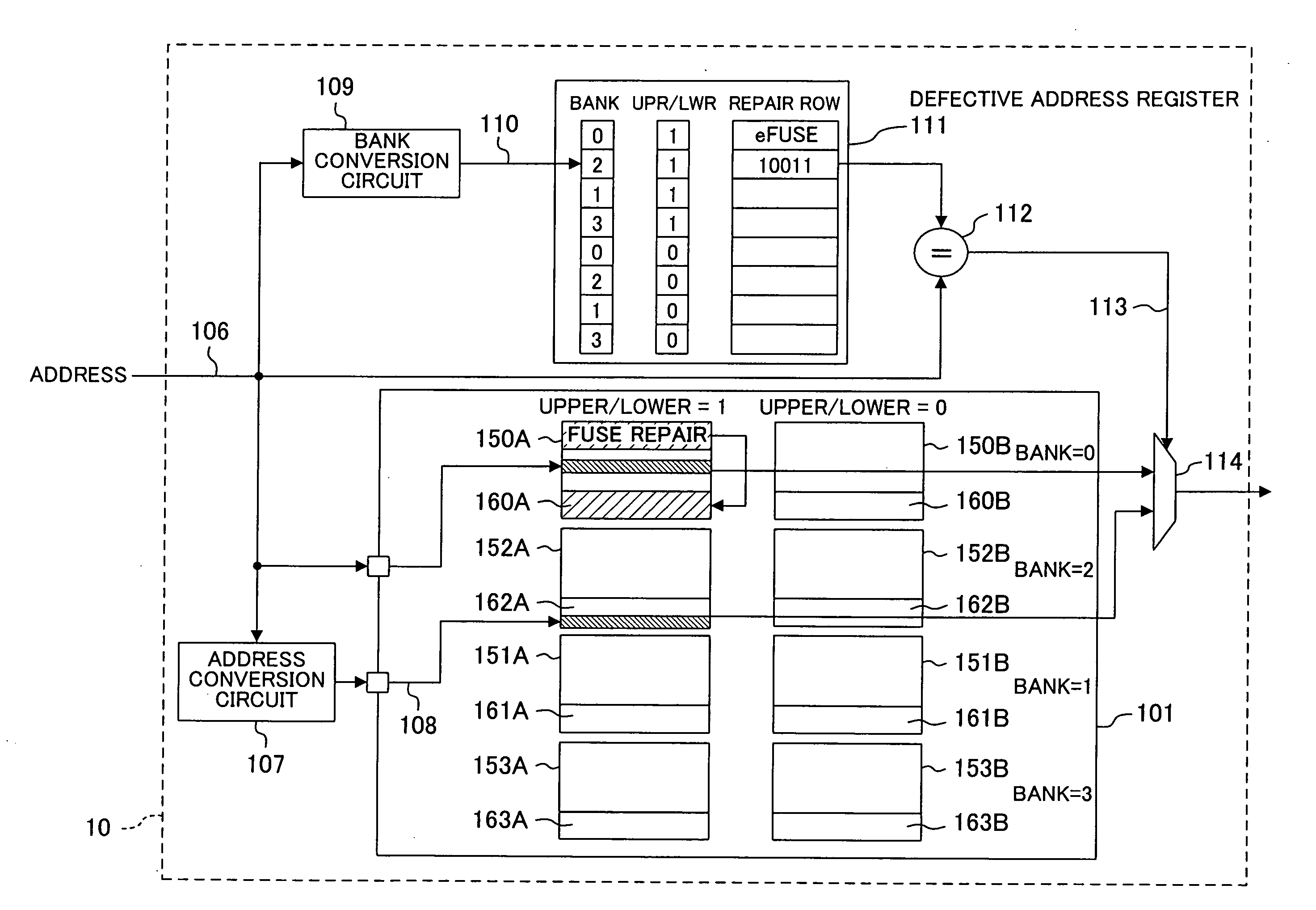
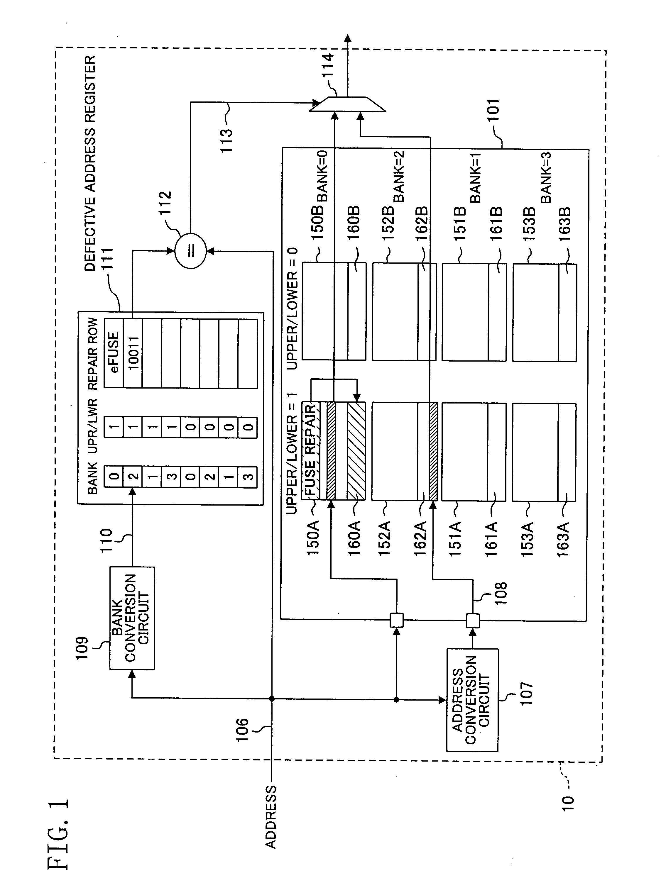
[0035]FIG. 1 is a block diagram showing a structure of a memory system 10 according to 20 the embodiment of the present invention. The memory system 10 of FIG. 1 includes a memory 101, an address conversion circuit 107, a bank conversion circuit 109, a defective address register 111; a hit signal generation circuit 112; and a selector 114. The memory system 10 receives an input address 106 given in the event of an access, reads data from the memory 101, and outputs the read data.

[0036]The memory 101 has memory banks 150A, 150B, 151A, 151B, 152A, 152B, 153A, and 153B. To specify a vertical position, any of bank numbers 0, 1, 2, and 3 is used, while either of bank columns 1 and 0 is used to specify a horizontal position. By specifying any of the bank numbers and either of the bank columns, one of the memory banks is selected.

[0037]The memory banks 150A, 150B, 151A, 151B, 152A, 152B, ...


PUM


Abstract

A memory system includes a memory having memory banks each having a redundant region for repairing a defect. When a plurality of defects occur in one of the memory banks, at least one of the defects is repaired by using the redundant region of the memory bank with the defects and at least one other of the defects is repaired by using the redundant region of another of the memory banks.

Description

CROSS REFERENCE TO RELATED APPLICATIONS[0001]The teachings of Japanese Patent Application JP 2006-203856, filed Jul. 26, 2006, are entirely incorporated herein by reference, inclusive of the claims, specification, and drawings.BACKGROUND OF THE INVENTION[0002]The present invention relates to a memory system for repairing a defect in a memory.[0003]Semiconductor memories that have been fabricated are subjected to a screening test. When a memory is determined to have a defective region by the test and the defective region is repaired, a method is used in an access to a memory in which it is determined whether or not an address inputted indicates the defective region in the memory and, when the inputted address indicates the defective region, the inputted address is converted to indicate a redundant region in the memory. To enable an efficient redundancy repair in a memory, a redundancy repair apparatus for a memory which performs a repair on a per address basis, not on a per column or...

Claims


Application Information

Patent Timeline
IPC IPC(8): G06F11/16
CPCG11C29/808
Inventor OYAGI, MUTSUMINISHIKAWA, RYOTA
Owner PANASONIC CORP
Why Eureka
Try Eureka