Miniature sensor chip, especially for finger print sensors

a sensor and miniature technology, applied in the field of sensor chips, can solve the problems of sensor relative large dimensions, difficult to realize the above-mentioned requirements relating to size and electronic functionality, and unsuitable finger interface, etc., and achieve the effect of cost saving

Inactive Publication Date: 2008-02-07
IDEX BIOMETRICS ASA
View PDF18 Cites 22 Cited by
  • Summary
  • Abstract
  • Description
  • Claims
  • Application Information

AI Technical Summary

Benefits of technology

[0013] Since the sensor thus may be produced using standard processes for IC product

Problems solved by technology

The abovementioned requirements related to size and electronic functionality may be difficult to realize using standard packing techniques in which the silicon circuit is mounted in a plastic based or ceramic housing.
At the

Method used


Image

  • Miniature sensor chip, especially for finger print sensors
  • Miniature sensor chip, especially for finger print sensors
  • Miniature sensor chip, especially for finger print sensors

Examples


Embodiment Construction

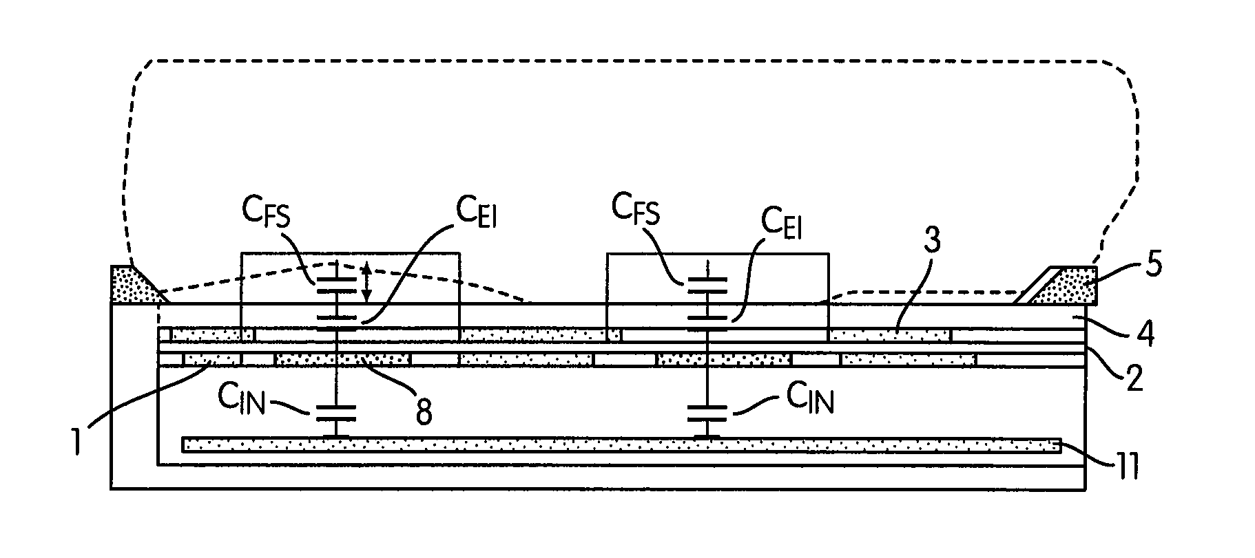
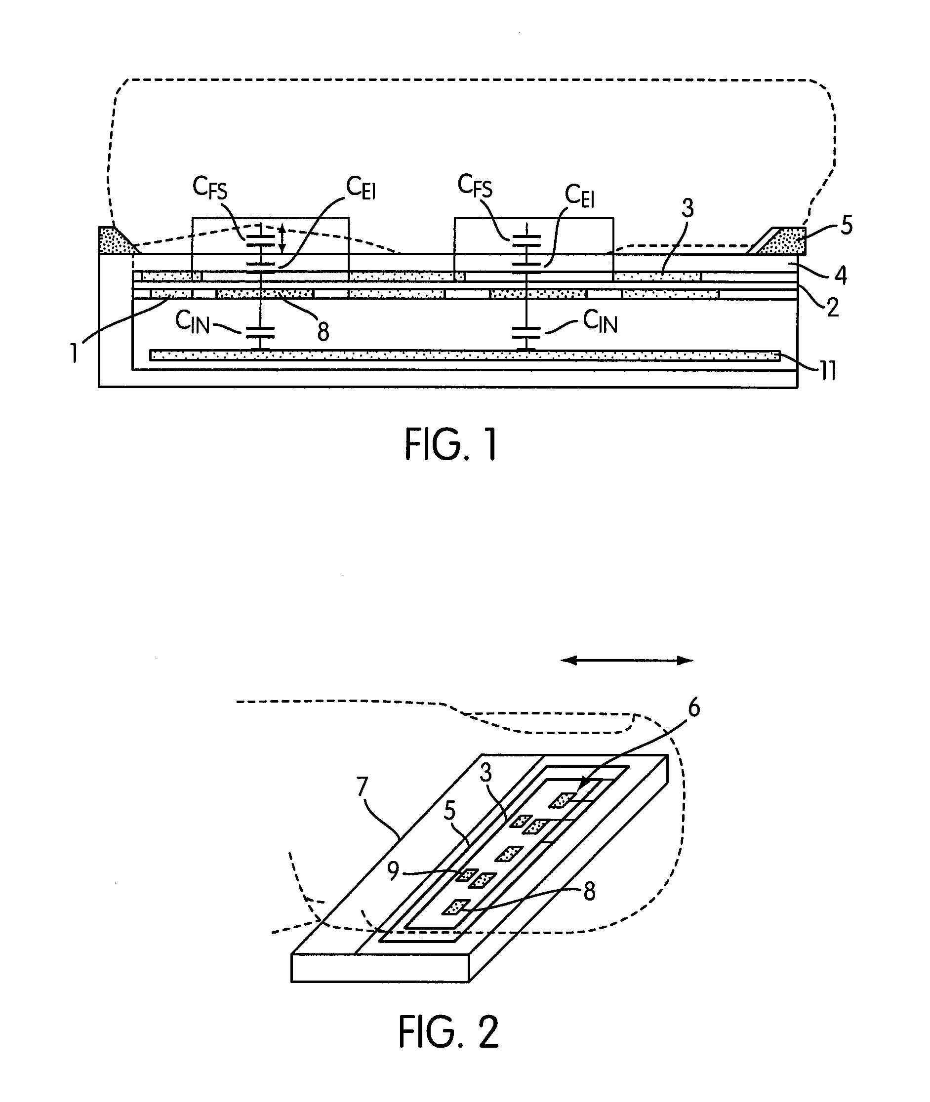
[0019] As is evident from the drawings the sensor chip according to the invention preferably consists of a naked silicon chip 6 in a housing 7 without a cover (or possibly on a circuit board or ceramic substrate) with a number of layers of metal or another electrically conductive material such as polysilicon, and a dielectric constituting the interface toward the user's fingers. The principle is based on imaging sensor elements constituting a part of the third or fourth upper layer of the electrically conductive layers 1 on the silicon circuit, and that the conductor lead, from the elements then is routed individually down to the amplifier circuits on the surface of the silicon chip.

[0020] The present solution may be produced industrially by standard methods for ASIC production and packing, as the silicon chip is mounted in a ceramic or plastic based housing without a lid, or on a circuit board or a ceramic substrate. The silicon chip is coupled electrically to the circuit board or...


PUM


Abstract

Sensor chip, especially for measuring of structures in a finger surface, characterized in that it comprises an electronic ship being in a per se known way provided with a number of sensor electrodes for capacitance measurements, the chip being provided with a first layer comprising a metal or another electrically conducting material over and coupled to the sensor electrodes and a first dielectric layer substantially covering the first metal layer.

Description

CONTINUITY [0001] This application is a continuation of U.S. application Ser. No. 10 / 297,745 filed Apr. 28, 2003, which is a 371 national phase of PCT / NO01 / 00239 filed Jun. 8, 2001, which claims priority to NO 20003003 filed Jun. 9, 2000, the respective disclosures of which are hereby incorporated by reference.BACKGROUND AND SUMMARY [0002] This invention relates to a sensor chip, especially for measuring structures in a finger surface. [0003] Fingerprint sensors based on capacitive coupling of an AC signal from the groove pattern of the finger to an array (matrix) of sensor elements are known from international patent application No PCT / NO98 / 00182. U.S. Pat. No. 5,963,679 describes a similar sensor with a different measuring principle and a two dimensional sensor matrix. [0004] For special applications, e.g. when being mounted in a cellular phone or a lap-top PC, it is important that the sensor is made as small and light as possible. Such a miniature sensor may also be very cost eff...

Claims


Application Information

Patent Timeline
IPC IPC(8): G01R27/26G01B7/28A61B5/117G01N27/22G06K9/00G06T1/00
CPCG06K9/00026G06K9/0002G06V40/1335G06V40/1306
Inventor VERMESAN, OVIDIUNYSAETHER, JONJOHANSEN, IB-RUNETSCHUDI, JON
Owner IDEX BIOMETRICS ASA
Why Eureka
Try Eureka