Multi-layered printed circuit board

Inactive Publication Date: 2008-02-07
SAMSUNG ELECTRONICS CO LTD
View PDF3 Cites 22 Cited by
  • Summary
  • Abstract
  • Description
  • Claims
  • Application Information

AI Technical Summary

Benefits of technology

[0032]According to another aspect of the invention, the heat sink is of electrically conductive material disposed on the multi-layered substrate over the signal lines. In this respect, the heat sink may consist of a plate of electrically conductive material tha

Problems solved by technology

Therefore, today's PCBs are correspondingly complex.
However, dual-sided and multi-layered PCBs are now being widely used today because the circuitry of today's electronic devices is more complex, more highly integrated and more compact than in the past.
In particular, errors that occur in the circuitry and interference between signals transmitted through the wires tend to become worse as the frequency becomes higher.
Therefore, the signal lines and the ground voltage layer present difficulties in incorporating these additional signal lines and components into the PCB.
However, a PCB having a micro strip line poses problems because the ground voltage layer is provided on the lower surface of the substrate.
Specifically, a PCB having a micro strip line suffers from a fringing phenomenon in which signals leak into the surrounding air and can produce undesired cross talk (in which the energy of a signal transmitted through a signal line leaks into an adjacent signal line).
That is, a PCB having a micro strip line experiences significant transmission loss.
However, designing a PCB so as to have a strip line is more difficult than designing a

Method used


Image

  • Multi-layered printed circuit board
  • Multi-layered printed circuit board
  • Multi-layered printed circuit board

Examples


first embodiment

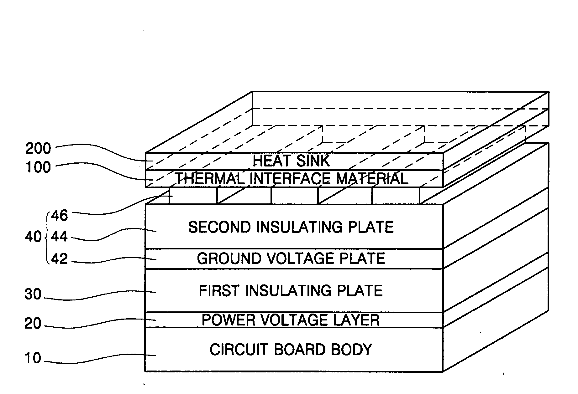
[0043]Referring to FIG. 3, a multi-layered PCB according to the present invention comprises a circuit board body 10, a power voltage layer 20, a first insulating plate 30, a multi-layered substrate 40, thermal interface material 100, and a heat sink 200 attached to the thermal interface material 100. The multi-layered substrate 40 comprises a ground voltage plate 42, a second insulating plate 44, and a plurality of signal lines 46. Three signal lines 46 are shown in FIG. 3 for clarity, but four or more signal lines can extend over the circuit substrate. Also, vias connect the circuit patterns on the various layers to each other.

[0044]The circuit board body 10, the power voltage layer 20, the first insulating plate 30, and the multi-layered substrate 40 (ground voltage layer 42, the second insulating plate 44 and the signal lines 46) are similar to those of FIG. 1. Thus, these elements will not be described in further detail for the sake of brevity.

[0045]The heat sink 200 preferably ...

second embodiment

[0050]FIG. 4 illustrates a multi-layered PCB according to the present invention. The multi-layered PCB of FIG. 4 comprises a circuit board body 10, a power voltage layer 20, a first insulating plate 30, a multi-layered substrate 40, a plurality of active electronic elements 300, thermal interface material 100, and a heat sink 200. The multi-layered substrate 40 comprises a ground voltage plate 42, a second insulating plate 44, and a plurality of signal lines 46.

[0051]The circuit board body 10, the power voltage layer 20, the first insulating plate 30, the multi-layered substrate 40, the thermal interface material 100, and the heat sink 200 are similar to those of the embodiment of FIG. 3. Thus, these elements will not be described in further detail for the sake of brevity. Also, three signal lines 46 and a single active element 300 are shown in FIG. 4 for the sake of clarity, but the PCB of the embodiment of FIG. 4 may have four or more signal lines 46 and has two or more active ele...

third embodiment

[0056]FIG. 5 illustrates a multi-layered PCB according to the present invention. The multi-layered PCB of FIG. 5 comprises a circuit board body 10, a power voltage layer 20, a first insulating plate 30, a multi-layered substrate 40, a plurality of active elements 300, thermal interface material 100, a heat sink 200, a third ground voltage plate 400, a clip 600, and a via 500 the multi-layered substrate 40 comprises a first ground voltage plate 42, a second insulating plate 44, and a plurality of signal lines 46. Although three signal lines 46 and a single active element 300 are shown in FIG. 5, the PCB may have four or more signal lines 46 and has two or more active elements 300. The thermal interface material 100 may bond the heat sink 200 to the signal lines and / or to the active elements 300. Also, the PCB has other vias connecting the circuit patterns on the various layers to each other.

[0057]The power voltage layer 20, the first insulating plate 30, the multi-layered substrate 4...


PUM


Abstract

A printed circuit board (PCB) has a multi-layered substrate including a plurality of signal lines and a ground voltage plate disposed below the signal lines and by which a common ground voltage is applied to the signal lines, a heat sink disposed on the multi-layered substrate, and thermal interface material interposed between the signal lines and the heat sink to transfer heat from the multi-layered substrate to the heat sink. The heat sink thus dissipates the heat generating from the multi-layered substrate and along with the ground voltage plate suppresses electromagnetic interference of signal transmitted through adjacent ones of the signal lines. The thermal interface material also serves in the design phase as a means to tune the impedance of the signal lines.

Description

BACKGROUND OF THE INVENTION[0001]1. Field of the Invention[0002]The present invention relates to a printed circuit board (PCB). More particularly, the present invention relates to multi-layered PCBs having strip lines and micro strip lines.[0003]2. Description of the Related Art[0004]Electronic devices typically include printed circuit boards (PCB) on which components that control the devices are mounted. Printed circuit boards (PCBs) are becoming smaller as the electronic devices are scaled-down to meet the demand for compact electronic devices, e.g., for portable electronic devices. Also, today's electronic devices have many functions and transmit data at high speeds. Therefore, today's PCBs are correspondingly complex.[0005]A PCB can be classified as a single-sided PCB in which wire (circuit) patterns are formed on only one side of an insulating substrate, a dual-sided PCB in which wire (circuit) patterns are formed on both sides of an insulating substrate, and a multi-layered PC...

Claims


Application Information

Patent Timeline
IPC IPC(8): H05K7/20
CPCH01L2224/16225H05K1/0203H05K1/0216H05K1/025H05K2201/066H05K1/0298H05K2201/0191H05K2201/0209H05K1/0259H01L2924/00011H01L2924/00014H01L2224/0401H05K3/46H05K7/20
Inventor KOO, CHANG-WOOLEE, JIN-SOOKKIM, DO-HYUNGYOO, HYUN-JUNG
Owner SAMSUNG ELECTRONICS CO LTD
Why Eureka
Try Eureka