Timing analysis method and device

a timing analysis and timing technology, applied in the field of semiconductor integrated circuits, can solve the problems of accumulating delay of instances (circuits including one or more logic circuits) forming paths, affecting the timing accuracy of timing analysis, and prolonging the period required for design and development. , to achieve the effect of improving timing convergence and reducing the amount of data

Inactive Publication Date: 2008-02-07
FUJITSU SEMICON LTD
View PDF11 Cites 28 Cited by
  • Summary
  • Abstract
  • Description
  • Claims
  • Application Information

AI Technical Summary

Benefits of technology

[0009] A timing analysis method and device capable of reducing the amount of data and analysis operation

Problems solved by technology

In the analysis method described above, however, variation in delays of instances (circuits including one or more logic circuits) forming a path is accumulated in accordance with the propagation order of a signal.
This makes the timing error convergence difficult and prolongs the period required for design and development.
However, this method does not take into account variation distributions caused by characteristics unique to the

Method used


Image

  • Timing analysis method and device
  • Timing analysis method and device
  • Timing analysis method and device

Examples


first embodiment

[0034] A timing analysis method according to the present invention will now be discussed with reference to the drawings.

[0035]FIG. 2 is a flowchart illustrating timing analysis performed by a timing analysis device 11 shown in FIG. 5.

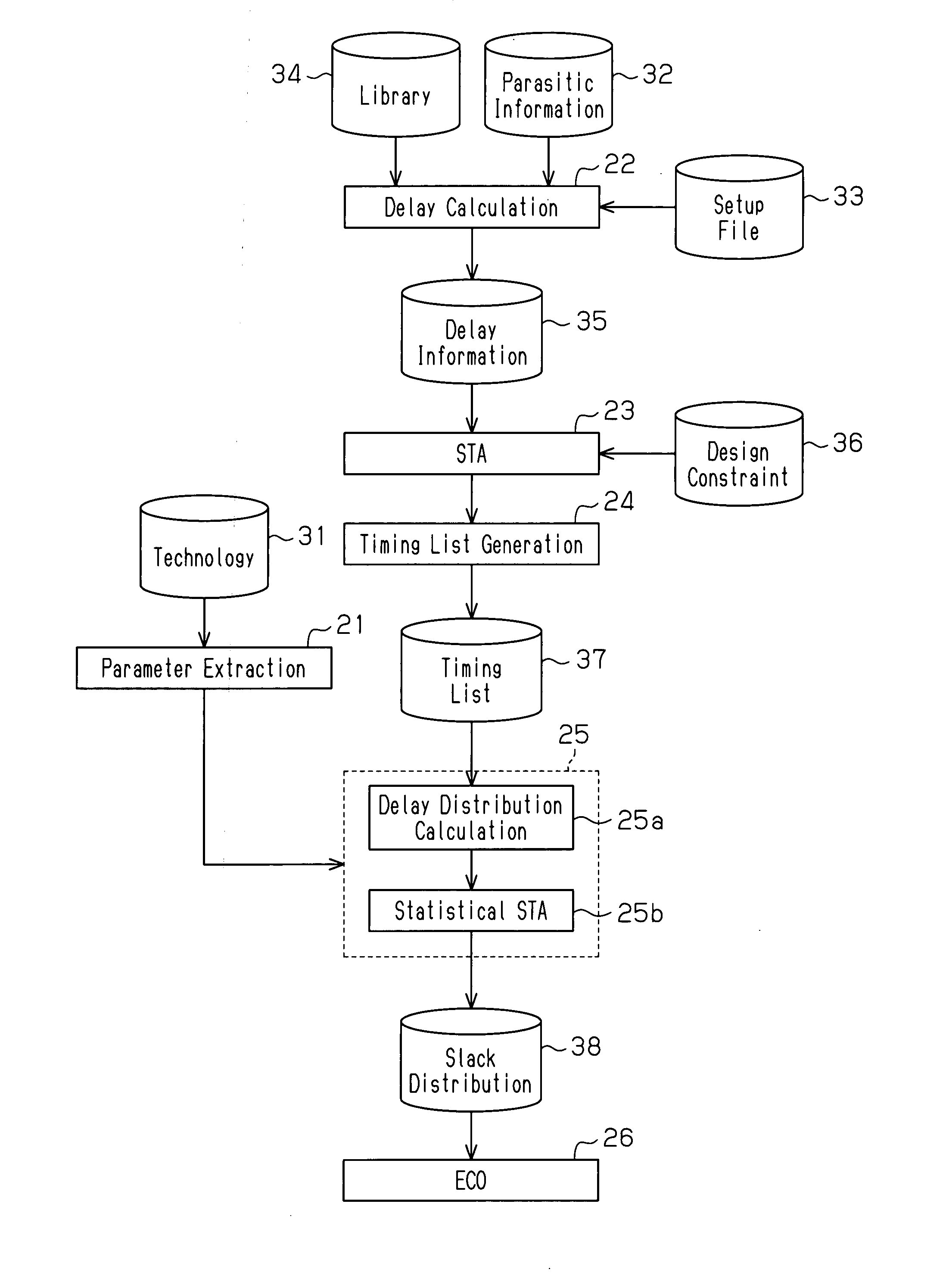
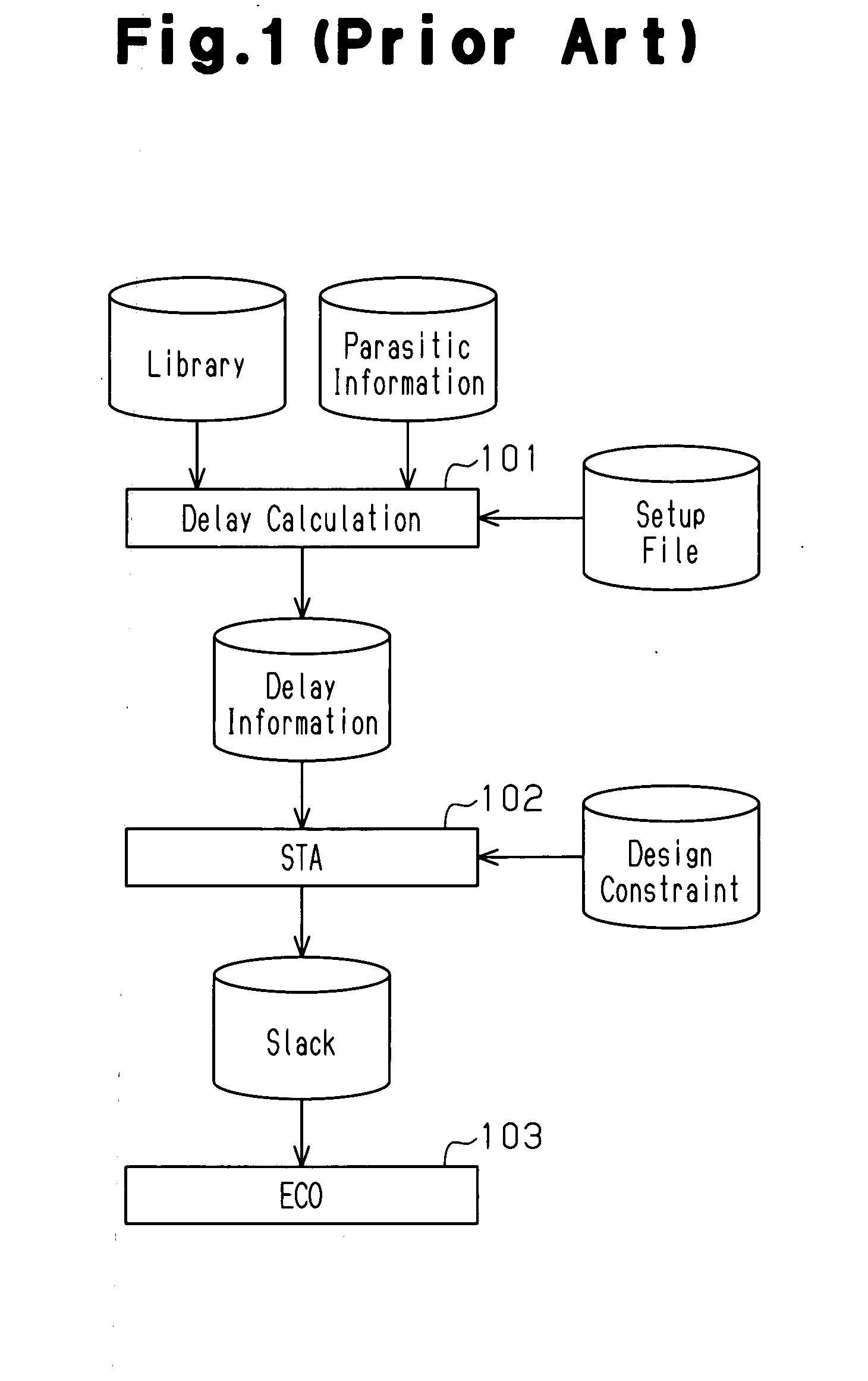
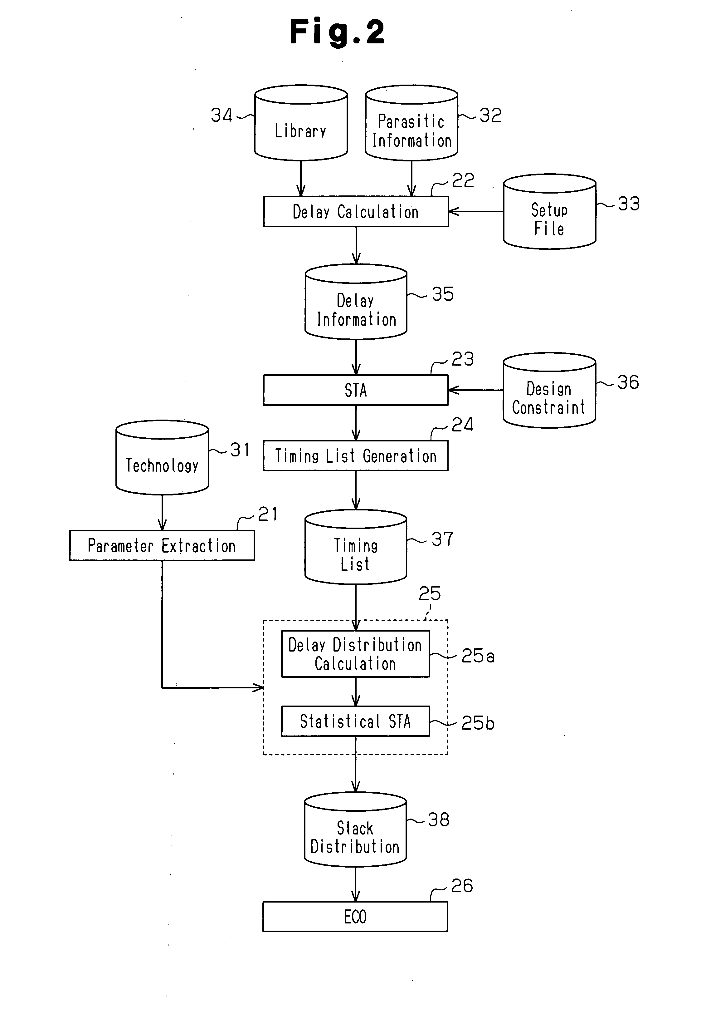
[0036] In step 21, the timing analysis device 11 simulates and analyzes delay time characteristics for each cell and each path based on a technology file 31. The timing analysis device 11 then generates a distribution parameter table using input slew rate and output load capacitance of each cell as parameters so that the table indicates distribution of the median values of delays and the delay variation amount (standard deviation) in accordance with these parameters. The technology file 31 contains system correction coefficients and variation characteristic values of delay time at the rising edge and falling edge of an output signal from each cell in a standard process. The system correction coefficients include a coefficient depending on the density o...

second embodiment

[0083] A timing analysis method according to the present invention will now be described with reference to the drawings.

[0084]FIG. 13 is a schematic flowchart showing a timing analysis process of the second embodiment. In the same manner as the first embodiment, the timing analysis process shown in FIG. 13 is performed by the timing analysis device 11 shown in FIG. 5.

[0085] Steps 201 to 204 of the timing analysis process in the second embodiment are identical to steps 21 to 24 of the timing analysis process in the first embodiment (refer to FIG. 2). Therefore, steps 201 to 204 will not be described in detail.

[0086] In a reanalysis process (step 205), the timing analysis device 11 reads the information of the timing list 37 generated in step 204.

[0087] The timing list 37 includes information of a path under relatively strict timing conditions. The path is a signal propagation path and includes path information and information of two points (start point and end point) defining the ...


PUM


Abstract

A timing analysis device for preventing the amount of data and the number of analysis operations from increasing in a statistical analysis, while improving the timing convergence in a path included in a net under relatively strict timing conditions. The timing analysis device performs a static timing analysis to extract a net under relatively strict timing conditions from the analysis result and generate a timing list. The device further performs delay distribution calculation for the extracted net to analyze the delay variation in each of one or more instances included in the net. The device retrieves the timing list and sets a unique delay variation for each instance to calculate a delay distribution. The device further performs a statistical timing analysis based on the calculated delay distribution.

Description

CROSS-REFERENCE TO RELATED APPLICATIONS [0001] This application is a continuation-in-part application of pending U.S. patent application Ser. No. 11 / 396,540 filed on Apr. 4, 2006, entitled “TIMING ANALYSIS METHOD AND DEVICE”.BACKGROUND OF THE INVENTION [0002] It is related to a semiconductor integrated circuit, and more particularly, to a method and device for efficiently analyzing timing in a digital circuit. [0003] In a development process for semiconductor integrated circuits, static timing analysis (STA) is performed to verify timing in digital circuits. The static timing analysis verifies the timing in a circuit based on delay times assigned to elements in the circuit. In addition to the static timing analysis, a statistical analysis technique has recently been introduced to analyze timing. For timing verification employing this statistical analysis technique, there is a demand for improving timing convergence in a path (signal propagation path) included in a net under relative...

Claims


Application Information

Patent Timeline
IPC IPC(8): G06F17/50
CPCG06F17/5031G06F30/3312
Inventor HOSONO, TOSHIKATSU
Owner FUJITSU SEMICON LTD
Why Eureka
Try Eureka