

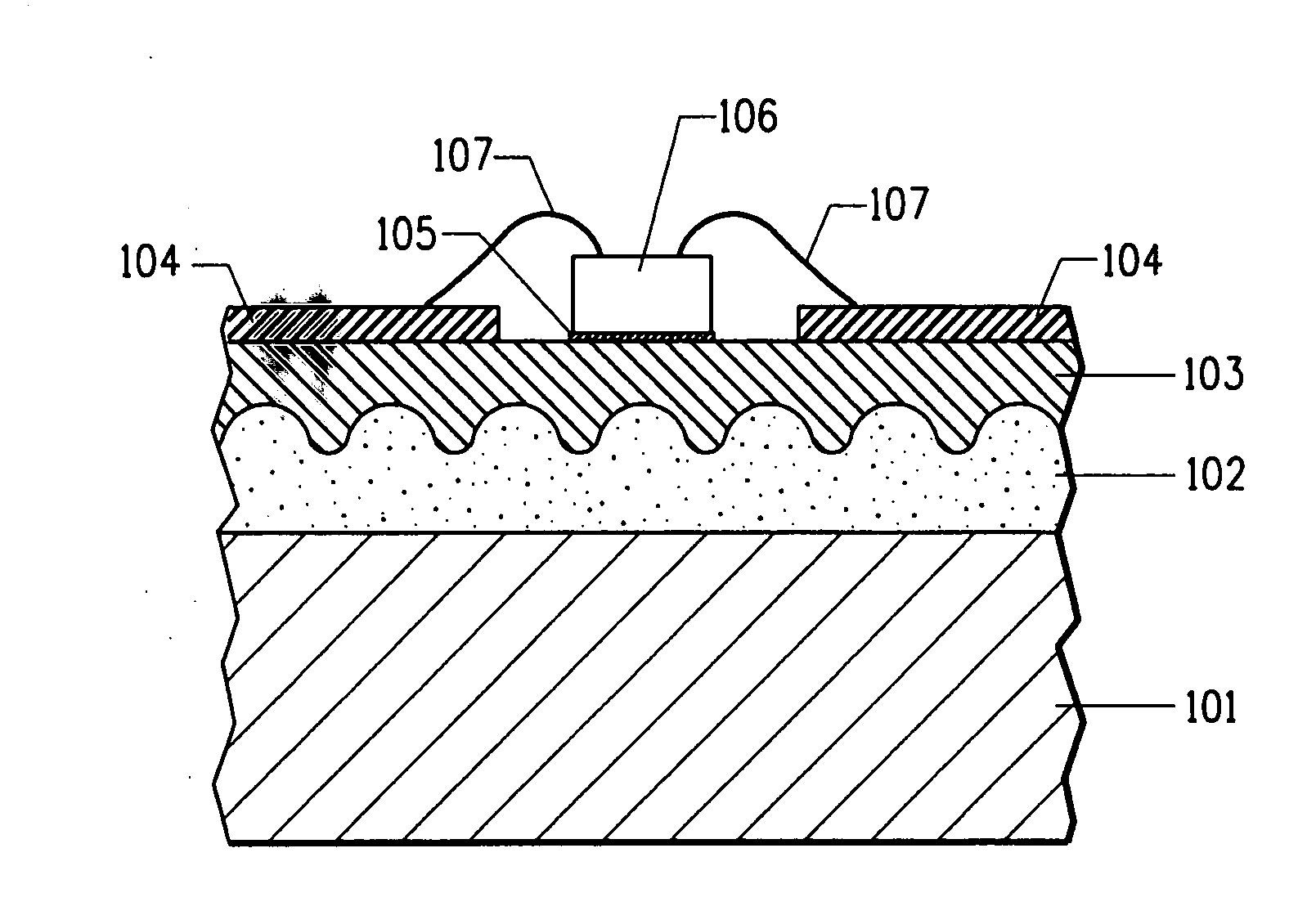
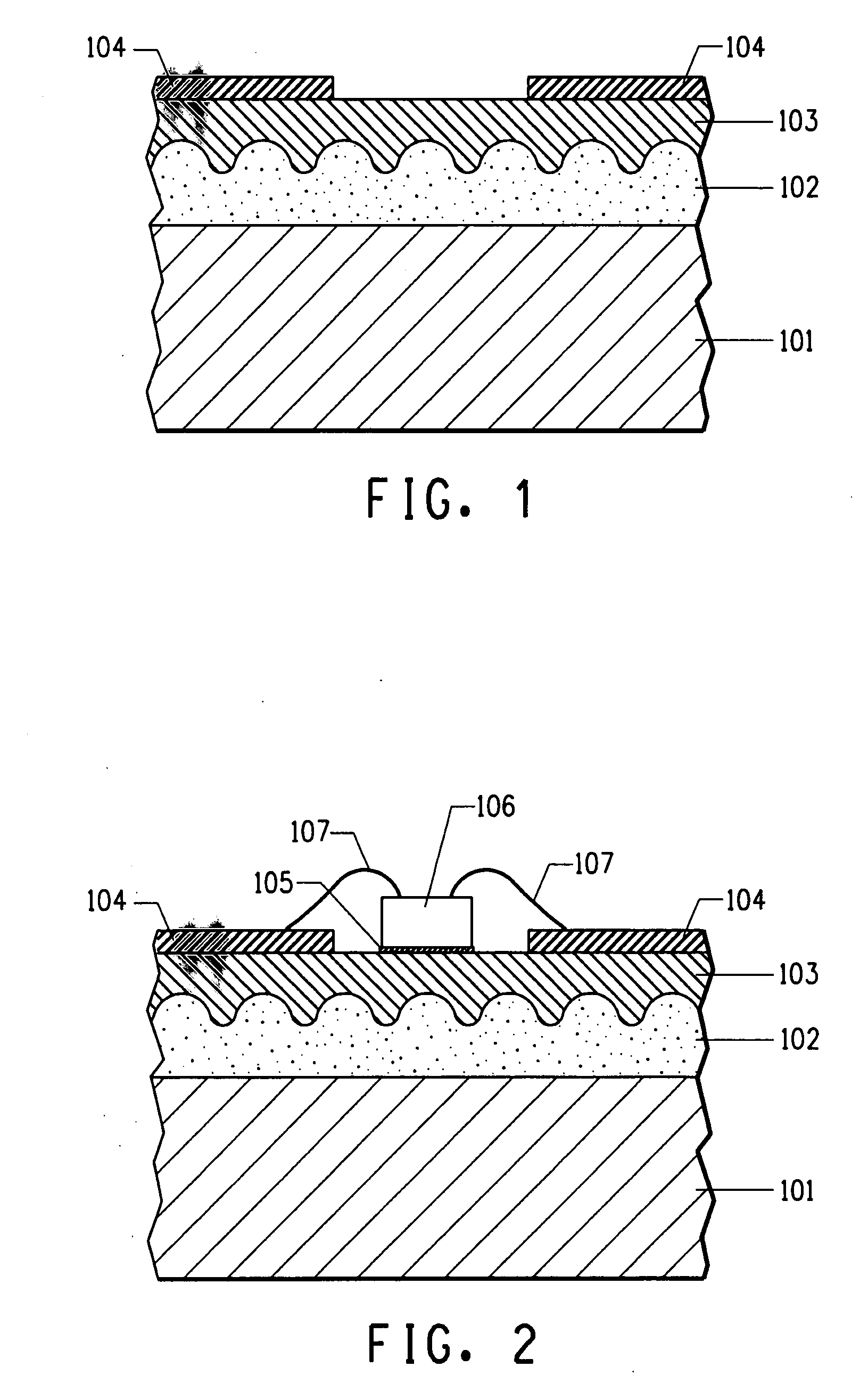
Device chip carriers, modules, and methods of forming thereof
a chip carrier and module technology, applied in the direction of printed circuit manufacturing, printed circuit aspects, basic electric elements, etc., can solve the problems of not being existing technology or materials may not be able to withstand high heat applications, and printed circuit board designs are typically formed
- Summary
- Abstract
- Description
- Claims
- Application Information
AI Technical Summary
Benefits of technology
Problems solved by technology
Method used
Image

Examples
examples
[0043]The present invention will be described in further detail by giving practical examples. The scope of the invention, however, is not limited in any way by these practical examples.
examples 1 through 17
[0044]The purpose of these experiments was to evaluate two separate DuPont experimental thick film compositions provided by E.I. du Pont de Nemours and Company, Dielectric A and Dielectric B, on anodized aluminum substrates (base material with an anodized aluminum upper surface). These dielectric compositions were thick film dielectric paste compositions. Each Dielectric A and B was tested with 4 different conductive layers (i.e., Silver A, B, C, and D). Additionally, each dielectric, Dielectric A and B, were once fired and twice fired, then both the once fired and twice fired dielectrics were tested with each of the 4 different conductive layers, thus giving 16 Examples total. A control, Example 17, with no dielectric layer was also conducted.
[0045]The substrates were cut 1″×1″, 40 mil thick anodized aluminum supplied by Nimet Industries, Inc. This anodized aluminum base material comprised an anodic film upper surface layer (i.e., an anodized aluminum surface). The anodic film was ...
examples 18-27
[0054]Hardcoat Anodized Al-3003 [Oxidized Al—This is same anodized substrate as used in previous experiments, Examples 1-16, above.]
[0055]Judgment of good and bad compositions were determined by looking at the Overall Cosmetics (mudcracking, roughness, blistering, etc) with special emphasis on mudcracking and blistering or bubbling. “Bubbling” is defined herein as an outgassing phenomenon and / or sintering phenomenon wherein a void or porous pocket is left in the fired film and leaves the film susceptible to low breakdown voltage and shorts. Another cosmetic dielectric is dewetting of the composition on the oxide layer. Any of these cosmetic defects were evaluated and if present were used to eliminate a dielectric composition candidate even before further electrical testing (shorting and breakdown voltage) was evaluated.
[0056]With the Hardcoat anodized Al-3003 (thickness of 40 mils) several compositions, did not succeed. The compositions listed in the following table did not give pro...
PUM
 Abstract
Description
Claims
Application Information