Array Panel

Active Publication Date: 2008-02-14
AU OPTRONICS (SUZHOU) CORP LTD
View PDF16 Cites 18 Cited by
  • Summary
  • Abstract
  • Description
  • Claims
  • Application Information

AI Technical Summary

Benefits of technology

[0013]With the above arrangements, the invention can improve the color washout problem under wide viewing angles and further achieve an ideal arrangement for liquid crystal cells to prevent light leakage from occurring. As a result, there is a better display quality.

Problems solved by technology

However, the display that employs the multi-domain alignment technique has problems involving color washout under wide viewing angles and light leakage.
These complications have led to alterations in the manufacturing process, resulting in higher costs.
Still, due to the irregular distribution of the electric field, the neighboring liquid crystal cells of the two pixel structures are not well arranged.
These improperly arranged liquid crystal cells leads to color washout, such that a brightness area distribution is irregular, especially for representing left and right viewing angles.
Consequently, although the PSA technique has enhanced the contrast ratio and brightness, while shortening the response time for TFT LCDs, the color washout problem under a wide viewing angle still has not been resolved.
In addition, the brightness area distribution is not uniform due to the irregular arrangement of the liquid crystal cells which causes light leakage and affects display quality.

Method used


Image

  • Array Panel
  • Array Panel
  • Array Panel

Examples


first embodiment

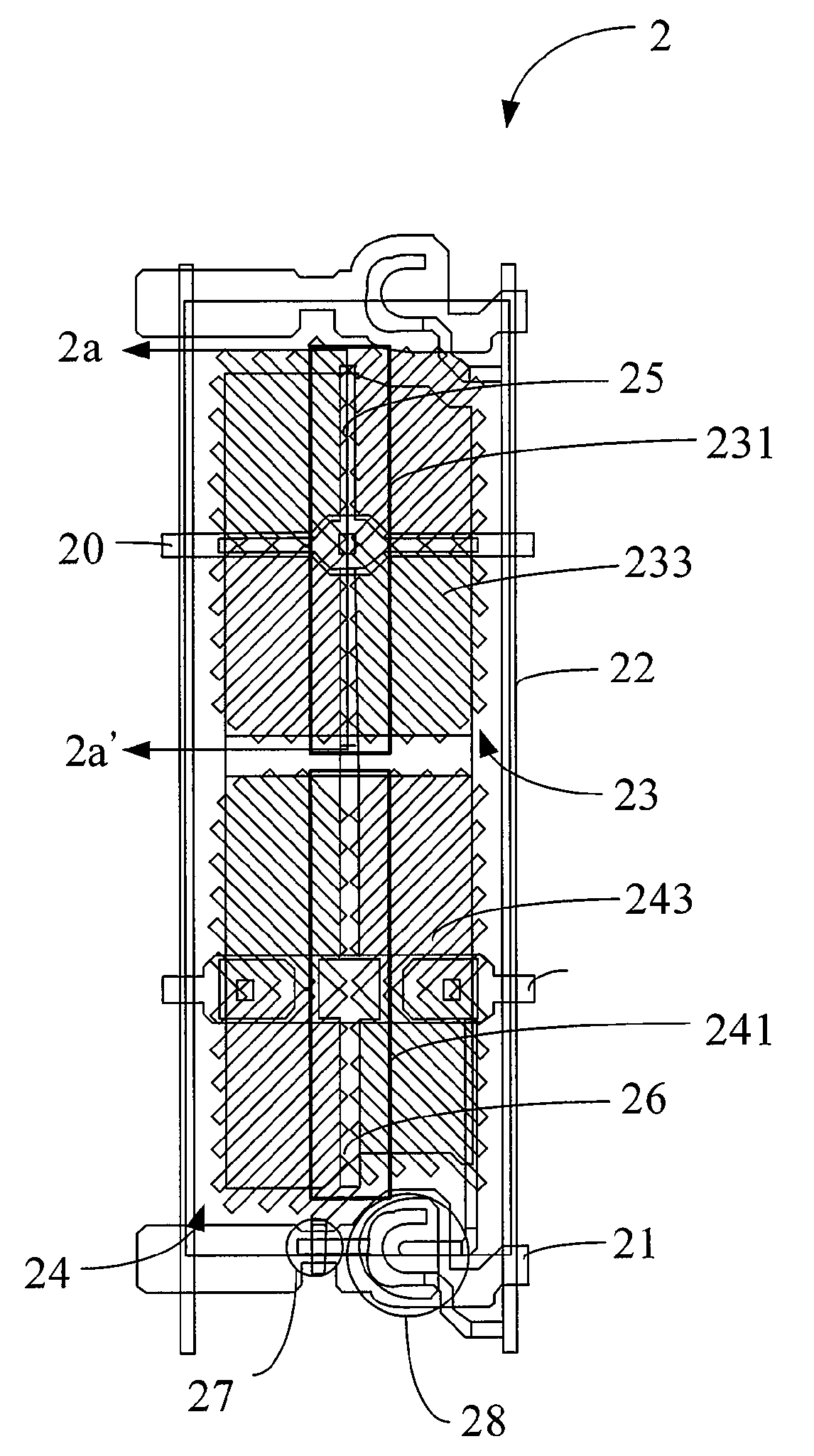
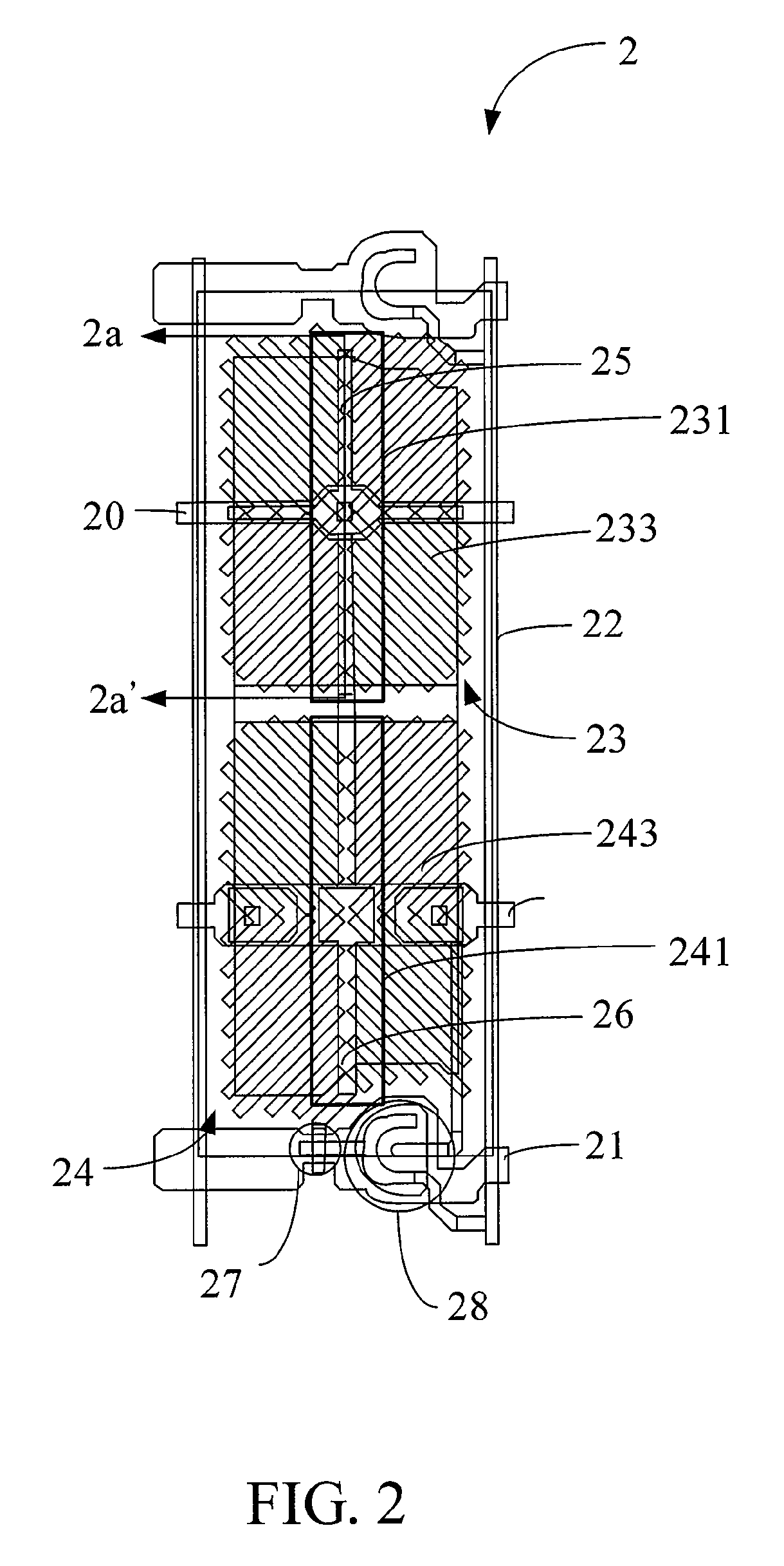
[0027]the invention is shown in FIG. 2 and FIG. 3. In this embodiment, a pixel structure 2 comprises a common electrode 20, a scan line 21, a data line 22, a first pixel electrode 23, a second pixel electrode 24, a first shield, a second shield, a first switch and a second switch. The first shield is a first conducting wire 25, electrically connected to the first pixel electrode 23. The first conducting wire 25 connects with a second conducting wire 26, so that both are electrically connected with a first TFT 27. The first TFT 27 is used to control the first pixel electrode 23. The first conducting wire 25 and the second conducting wire 26 can be formed simultaneously. The first switch and the second switch are the first TFT 27 and a second TFT 28, respectively. The content disclosed in Taiwan Patent Application No. 95129118 is incorporated herein by reference.

[0028]FIG. 2 is an upper view of a pixel structure 2 of a first embodiment of the invention, while FIG. 3 is a cross-section...

second embodiment

[0034]the invention is shown in FIG. 5. In this embodiment, a pixel structure 5 comprises a scan line 51, a data line 52, a first pixel electrode 53, a second pixel electrode 54, a first switch, and a second switch, wherein the first switch and the second switch are the first TFT 55 and the second TFT, respectively. The scan line 51 is used to transmit a scan signal, while the data line 52 is used to transmit a voltage signal.

[0035]The first pixel electrode 53 comprises a first central portion 531, a plurality of branches 533, a first connecting portion 535, and first auxiliary connecting portions 537, 537′. The first connecting portion 535 and the first auxiliary connecting portion 537 may or may not connect together. The plurality of branches 533 connects with the first central portion 531. Preferably, the plurality of branches 533 extends along the direction of an included angle, which can range from either 40°˜50°, 130°˜140°, 220°˜230°, or 310°˜320° with the first central portio...

third embodiment

[0048]The third embodiment is only used to illustrate one aspect of the invention. Adjustments can be made in other embodiments. For example, either the width of the first branch can be equal to the width of the first common electrode, or the width of the second branch can be equal to the width of the second common electrode. The difference in width between the first branch of the first pixel electrode and the first common electrode is about 0 μm to 8 μm.

[0049]The invention further reveals an array panel used in a TFT LCD. The array panel comprises a substrate, a first common electrode, a second common electrode, and a plurality of pixel structures. Both the first common electrode and the second common electrode are disposed on the substrate, and the plurality of the pixel structures is also disposed on the substrate.

[0050]A fourth embodiment of the invention is shown in FIG. 8 which shows an upper view of a pixel structure 8. In this embodiment, the pixel structure 8 comprises a sc...


PUM


Abstract

An array panel is provided. The array panel comprises a substrate, a common electrode, and pixel structures. Each pixel structure comprises a first pixel electrode, a second pixel electrode, and a shield. The first pixel electrode has a central portion, first branches that connect to the central portion, and a connecting portion. The shield overlaps with at least the central portion of the first pixel electrode. The connecting portion connects the ends of at least two of the first branches. The central portion connects perpendicularly with one of the first branches; this branch overlaps with at least part of the common electrode so that the width of this branch is greater than or equal to that of the common electrode. The second pixel electrode, adjacent to the first pixel electrode, comprises a central portion and second branches that connect to the central portion.

Description

[0001]This application claims the benefit from the priority of Taiwan Patent Applications No. 095138272 filed on Oct. 17, 2006 and 095129118 filed on August 8, in which the disclosure of the latter is incorporated by reference herein in its entirety.BACKGROUND OF THE INVENTION[0002]1. Field of the Invention[0003]The present invention relates to an array panel, specifically, to an array panel of a liquid crystal display that a color washout problem is reduced or avoided when under a wide viewing angle.[0004]2. Descriptions of the Related Art[0005]With fast developing technologies, people have become accustomed to using various electronic products. One key component of multimedia electronic products is the display. Because of its desirable characteristics, such as power-saving, radiation-free, small size, low power consumption, space-saving, flat square, high resolution, and stable display quality, thin film transistor liquid crystal displays (TFT LCDs) have gradually started to repla...

Claims


Application Information

Patent Timeline
IPC IPC(8): H01J1/00
CPCG02F1/133707G09G2320/0233G02F1/13624G02F1/134309
Inventor CHAN, TE-WEIHUANG, YI-PAICHIU, CHUNG-YICHEN, YEN-TING
Owner AU OPTRONICS (SUZHOU) CORP LTD
Why Eureka
Try Eureka