Organic electroluminescent panel and production method thereof, and color filter substrate and production method thereof

a technology of electroluminescent panels and substrates, applied in the direction of discharge tubes/lamp details, discharge tubes luminescnet screens, electric discharge lamps, etc., can solve the problems of high production costs, insufficient production efficiency, and insufficient production efficiency, so as to achieve effective suppression of inflow of ink into adjacent pixels, high accuracy, and reduced discontinuity of upper electrodes

Active Publication Date: 2008-02-14
SHARP KK
View PDF14 Cites 46 Cited by
  • Summary
  • Abstract
  • Description
  • Claims
  • Application Information

AI Technical Summary

Benefits of technology

[0024] It is preferable that the bank satisfies a relationship of t2>t1×1.5 if a film thickness in a region having a relatively small film thickness (a first region) is defined as t1 and a film thickness in a region having a relatively large film thickness (a second region) is defined as t2. As a result, the inflow of the ink into the adjacent pixels can be effectively suppressed and simultaneously the discontinuity of the upper electrode can be effectively reduced. It is more preferable that the bank satisfies a relationship of t2>t1×3.0 for more remarkable functional effects of the present invention. The value of t1 or t2 is appropriately adjusted depending on film thickness of the organic layer, and the like. The lower limit of t1 is preferably 0.5 μm and the upper limit thereof is preferably 2.0 μm. The lower limit of t2 is preferably 1.5 μm and the upper limit thereof is preferably 10.0 μm.
[0025] It is preferable that a region having a relatively large film thickness (a second bank region) has a forward tapered cross-sectional shape. According to this embodiment, the droplet on the bank side surface is likely to slip and gather inside the bank. Therefore, the position where the ink is applied is controlled with high accuracy and the certainty of the patterning can be improved, and thereby the color mixing can be more effectively suppressed. The bank having a forward tapered shape means that the bank has a substantially trapezoidal cross-sectional shape having a wide lower side (the upper base is shorter than the lower base) when cut in the direction perpendicular to the substrate. It is more preferable that both of the bank having a relatively large film thickness (the second bank region) and the bank having a relatively small film thickness (a first bank region) have a forward tapered cross-sectional shape.
[0026] It is preferable that a region having a relatively large film thickness (a second bank region) is discontinuously formed. Thus, the bank having a relatively small film thickness (a first bank region) is formed in a priority at an intersection of the bank pattern of the region having a relatively large film thickness (the second bank region) with the bank pattern of the region having a relatively small film thickness (the first bank region) . As a result, in the upper electrode, the electricity flows in a lateral direction (the direction in which R, G, and B are positioned in FIG. 1), and the resistance value of the upper electrode can be effectively reduced.
[0027] The present invention is a production method of an organic electroluminescent panel comprising a lower electrode, a bank, an organic film, and an upper electrode on a sub

Problems solved by technology

Such organic electroluminescent displays are still inferior to liquid crystal displays (LCD) or plasma display panels (PDP) in technical completeness or standard of industrial infrastructure.
Therefore, film unevenness is likely to be generated in a large area panel, and production costs are high.
Therefore, no technical prospect of production process for large panels has yet emerged.
However, if the in

Method used


Image

  • Organic electroluminescent panel and production method thereof, and color filter substrate and production method thereof
  • Organic electroluminescent panel and production method thereof, and color filter substrate and production method thereof
  • Organic electroluminescent panel and production method thereof, and color filter substrate and production method thereof

Examples


embodiment 1

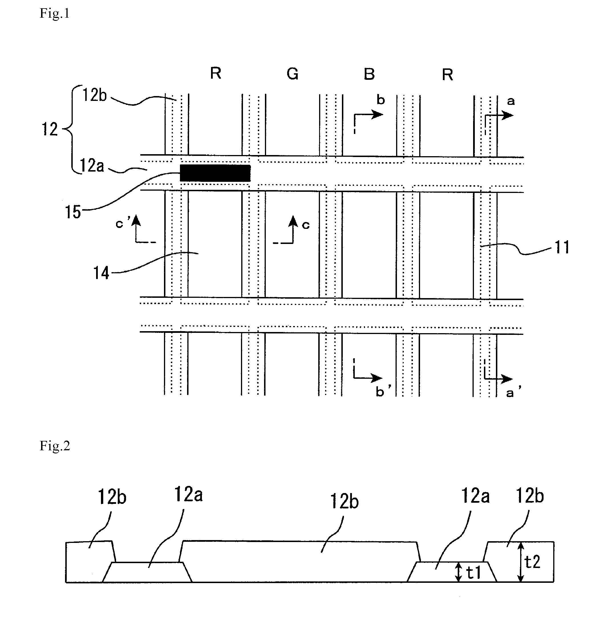
[0045]FIG. 1 is a front view schematically showing a configuration of an active matrix (AM) driving full-color organic electroluminescent (EL) display device in accordance with Embodiment 1 of the present invention. R, G, and B in FIG. 1 represent a red pixel, a green pixel, and a blue pixel, respectively.

[0046] The organic EL display device in accordance with the present Embodiment is designed with the AM driving. A lower electrode 11 serving as a pixel electrode is arranged in an island pattern where the electrodes are partitioned into each other on a dot basis (every pixel), and an upper electrode 13 is arranged as an electrode that is common to every pixel. Transparent conductive films of ITO (indium tin oxide) , IZO (indium zinc oxide), and the like are used as the lower electrode 11 in a bottom emission type in which light is emitted from the substrate side (the lower electrode side), and films of aluminum (Al), silver (Ag), platinum (Pt), nickel (Ni), or an alloy thereof are...

embodiment 2

[0060]FIG. 5 is a front view schematically showing a configuration of a passive matrix (PM) driving full-color organic electroluminescent (EL) display device in accordance with Embodiment 2 of the present invention. R, G, and B in FIG. 5 represent a red pixel, a green pixel, and a blue pixel, respectively.

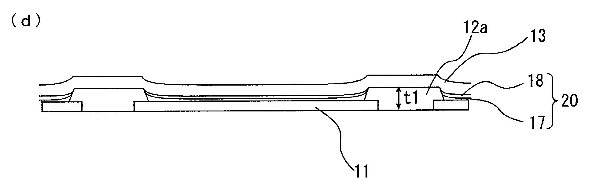
[0061] The organic EL display device in accordance with the present Embodiment is designed with the PM driving. The lower electrode 11 is arranged in a stripe pattern extending in the column direction (the vertical direction in FIG. 5), as shown in FIG. 5. The upper electrode (not shown) is arranged in a stripe pattern extending in the row direction (the lateral direction in FIG. 5). The pixel region 14 is surrounded by the bank 12 having two different forms (the first bank 12a and the second bank 12b).

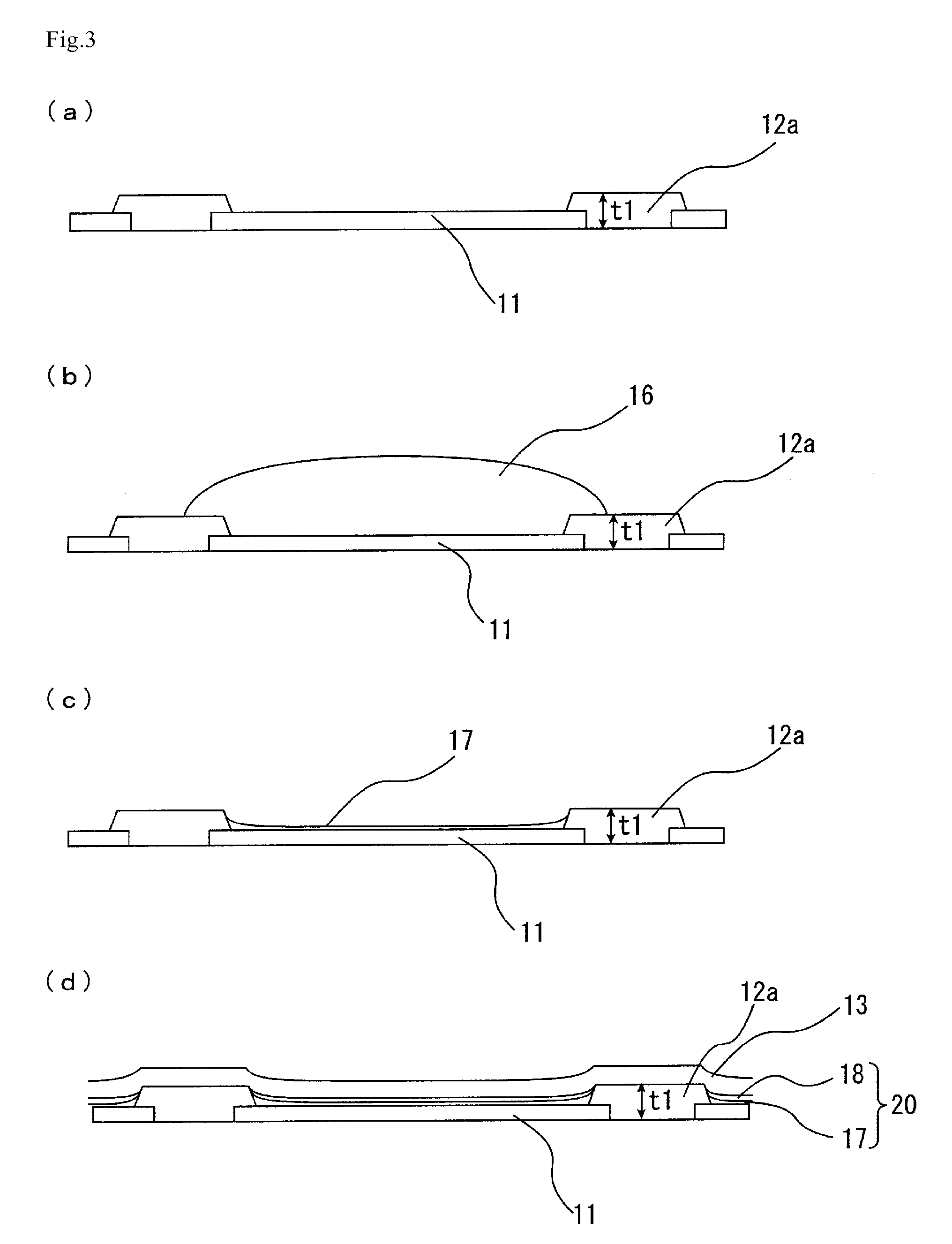
[0062] The production process flow of the organic EL display device in accordance with the present Embodiment is mentioned below.

[0063] First, the lower electrode 11 is formed in ...


PUM


Abstract

The present invention provides an organic electroluminescent panel, a production method thereof, and an organic electroluminescent display device, in which color mixing between adjacent pixels, caused by overflow or pull-in of a liquid material is suppressed and discontinuity (physical and electrical separation by the step) of an upper electrode is reduced when an organic film such as a luminescent layer is formed by an application method such as an ink jet printing method. The organic electroluminescent panel of the present invention is an organic electroluminescent panel comprising a lower electrode, a bank, an organic film, and an upper electrode on a substrate, wherein the organic electroluminescent panel has: two or more bank regions having different film thicknesses; and an organic film region surrounded by the two or more bank regions, the organic film region having a planar shape of a quadrangle or a substantial quadrangle with a rounded vertex or side.

Description

BACKGROUND OF THE INVENTION [0001] 1. Field of the Invention [0002] The present invention relates to organic electroluminescent panels and production methods thereof, and color filter substrates and production methods thereof. More specifically, the present invention relates to an organic electroluminescent panel preferable for large and full-color panels, a production method thereof, an organic electroluminescent display device, a color filter substrate, a production method thereof, a liquid crystal display panel, and a liquid crystal display device. [0003] 2. Description of the Related Art [0004] Organic electroluminescent (hereinafter, also referred to as “EL”) displays have been drawing attention as a next generation flat panel display (FPD) because such displays are excellent in visibility such as contrast and viewing angle and responsivity and permits low power consumption, slim profile, light weight, and flexibilization of the displays themselves. Such organic electroluminesc...

Claims


Application Information

Patent Timeline
IPC IPC(8): H05B33/00H01L51/50H05B44/00
CPCG02B5/20H01L51/0005H01L27/3283H01L27/3246H10K59/122H10K59/173H10K71/135H10K2102/351
Inventor OKANO, KIYOSHI
Owner SHARP KK
Why Eureka
Try Eureka