Electro-optical device, driving circuit, and electronic apparatus

a driving circuit and electronic equipment technology, applied in the direction of oscillator generators, pulse techniques, instruments, etc., can solve the problems of adverse display effect, inability to display the gray scale of pixels corresponding to the capacitor lines, complex configuration of the circuit that drives the capacitor lines, etc., to reduce the adverse display effect, simple configuration, and suppress the voltage amplitude of data lines

Active Publication Date: 2008-02-14
JAPAN DISPLAY WEST
View PDF5 Cites 30 Cited by
  • Summary
  • Abstract
  • Description
  • Claims
  • Application Information

AI Technical Summary

Benefits of technology

[0006]An advantage of some aspects of the invention is that it provides an electro-optical device that suppresses voltage amplitudes of da

Problems solved by technology

However, in this technology, because a circuit that drives the capacitor lines is similar to the scanning line driving circuit (actually, a shift register) that drives the scanning lines, the configuration of the circuit that drives the capacitor lines becomes complex.
In addition, if a voltage

Method used


Image

  • Electro-optical device, driving circuit, and electronic apparatus
  • Electro-optical device, driving circuit, and electronic apparatus
  • Electro-optical device, driving circuit, and electronic apparatus

Examples


first embodiment

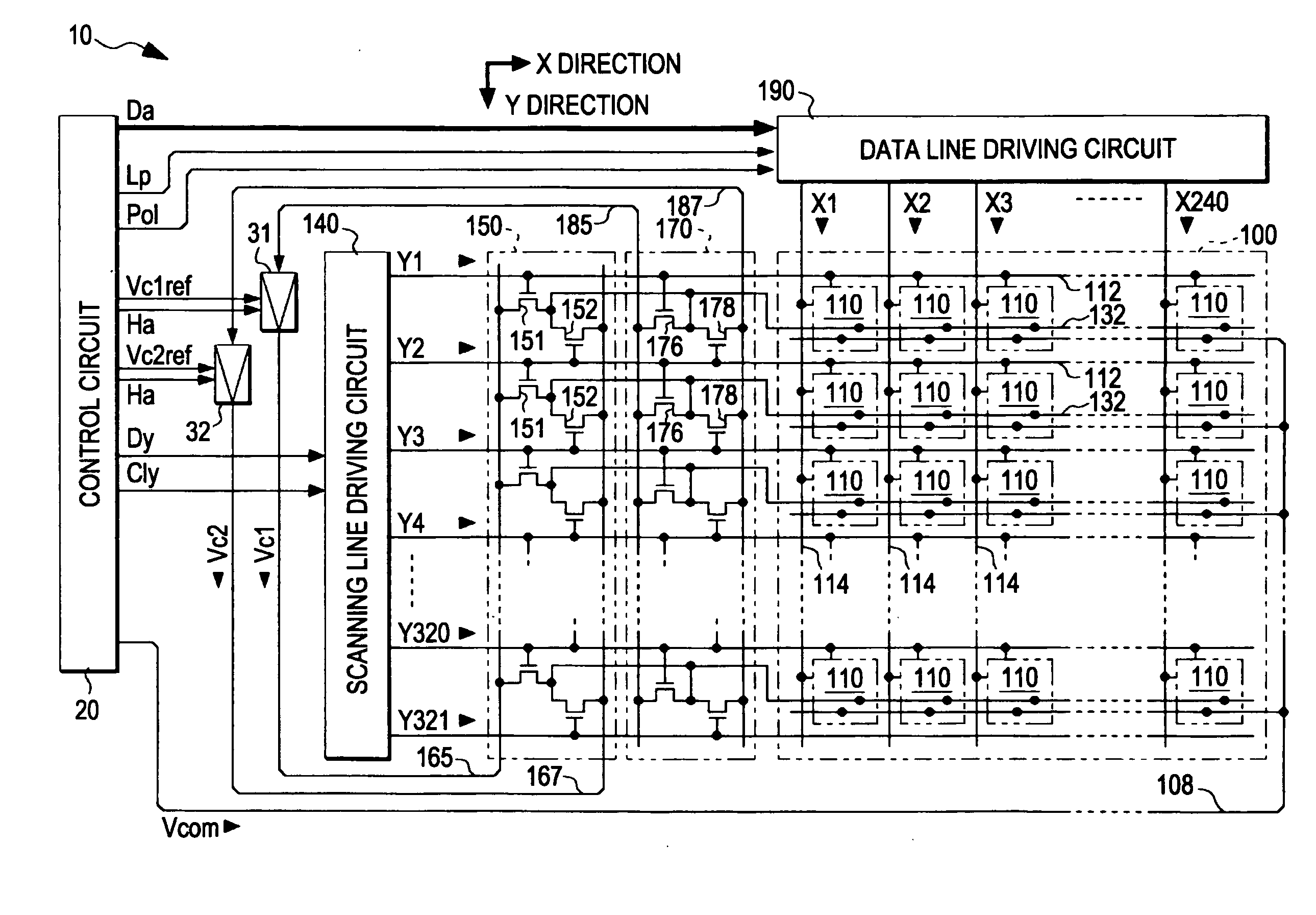
[0036]A first embodiment of the invention will now be described. FIG. 1 is a block diagram showing a configuration of an electro-optical device according to the first embodiment of the invention. As shown in the drawing, the electro-optical device 10 has a panel structure of peripheral circuit built-in type. The electro-optical device 10 includes a display area 100, a scanning line driving circuit 140, a capacitor line driving circuit 150, a detection circuit 170 and a data line driving circuit 190. These circuits 140, 150, 170, 190 are arranged around the display area 100. In addition, a control circuit 20, a first capacitive signal output circuit 31 and a second capacitive signal output circuit 32 form a circuit module, which is connected to the peripheral circuit built-in type panel by means of, for example, an FPC (flexible printed circuit) substrate.

[0037]The display area 100 is an area in which pixels 110 are arranged. In this embodiment, 321 scanning lines 112 (from first to ...

second embodiment

[0087]A second embodiment of the invention will now be described. FIG. 16 is a block diagram showing a configuration of an electro-optical device according to the second embodiment of the invention. The configuration shown in the drawing mainly differs from those of the first embodiment (see FIG. 1) in that capacitors 179 are provided in correspondence with the rows in the detection circuit 170. Specifically, one ends of the capacitors 179 corresponding to the odd numbered (1, 3, 5, . . . , 319) rows are connected to the capacitor lines 132 in the corresponding rows and the other ends thereof are connected to the first detection line 186, while one ends of the capacitors 179 corresponding to the even numbered (2, 4, 6, . . . , 320) rows are connected to the capacitor lines 132 in the corresponding rows and the other ends thereof are connected to the second detection line 188. The control circuit 20 outputs a row specifying signal Oe that attains an H level when the scanning lines 11...

third embodiment

[0090]In the above described first and second embodiments, the i-th capacitor line 132, when the scanning signal Y(i+1) attains an L level after the end of selection of the (i+1)th row scanning line, enters a high impedance state and continues the high impedance state until the next scanning signal Yi attains an H level after the following one frame period elapses. The capacitor lines 132 intersect with (or are in proximity to) other wiring lines and combine with the other wiring lines through parasitic capacitances, so that fluctuation in voltage of these wiring lines tends to influence the capacitor lines 132 (except the example shown in FIG. 15). Then, a third embodiment in which stabilization of voltage is attempted without causing the capacitor lines 132 to enter into a high impedance state will be described.

[0091]FIG. 18 is a block diagram showing a configuration of an electro-optical device according to the third embodiment of the invention. As shown in the drawing, in the th...


PUM


Abstract

A driving circuit includes a plurality of scanning lines, a plurality of data lines, a plurality of capacitor lines, pixels, a scanning line driving circuit, a capacitor line driving circuit, a first capacitive signal output circuit, and a data line driving circuit. Each of the pixels includes a pixel switching element, a pixel capacitor, and a storage capacitor. The capacitor line driving circuit supplies a first capacitive signal to the capacitor line when the one scanning line is selected, and changes a voltage value of the first capacitive signal when a scanning line, located a predetermined number of scanning lines away from the one scanning line, is selected. The first capacitive signal output circuit adjusts and outputs a voltage of the first capacitive signal when the one scanning line is selected. The data line driving circuit supplies the pixels with data signals of voltages corresponding to gray scale levels.

Description

BACKGROUND[0001]1. Technical Field[0002]The present invention relates to a technology that suppresses a voltage amplitude of a data line with a simple configuration in an electro-optical device, such as a liquid crystal display.[0003]2. Related Art[0004]In an electro-optical device, such as a liquid crystal display, pixel capacitors (liquid crystal capacitors) are provided correspondingly at intersections of scanning lines and data lines. When the pixel capacitors need to be driven by alternating current, the voltage amplitudes of data signals have positive and negative polarities (bipolarity). For this reason, in a data line driving circuit that supplies data signals to the data lines, component elements need to have withstanding voltages corresponding to the voltage amplitudes. JP-A-2001-83943 has proposed a technology in which storage capacitors are provided in parallel with pixel capacitors, and capacitor lines, to which the storage capacitors are commonly connected in each row,...

Claims


Application Information

Patent Timeline
IPC IPC(8): G06F3/038H03B1/00
CPCG06F3/0412
Inventor YAMAZAKI, KATSUNORI
Owner JAPAN DISPLAY WEST
Why Eureka
Try Eureka