Magnetic memory device

a memory device and magnetic technology, applied in the field of magnetic memory devices, can solve the problems of increasing the writing speed of a given current, and achieve the effect of high resistance sta

Inactive Publication Date: 2008-02-14
CENT NAT DE LA RECHERCHE SCI +2
View PDF26 Cites 56 Cited by
  • Summary
  • Abstract
  • Description
  • Claims
  • Application Information

AI Technical Summary

Benefits of technology

[0015]According to a first aspect of the present invention there is provided a magnetic memory device comprising: first and second leads; a magnetoresistive multilayer structure arranged between said leads such that current is conducted from the first lead to the second lead through layers of said multilayer structure, said multilayer structure exhibiting a first, relatively high resistance state and a second, relatively low resistance state, said multilayer structure including a first ferromagnetic layer having a magnetic hard axis and a magnetic easy axis, and said multilayer structure being switchable between said first and second states; and characterised by a magnetic field source for controllably applying a magnetic field along the magnetic hard axis in the ferromagnetic layer independently of current flow through the multilayer structure for assisting switching of the multilayer structure between first and second states.

Problems solved by technology

In turn, this can lead to an increase in writing speed for a given current.

Method used


Image

  • Magnetic memory device
  • Magnetic memory device
  • Magnetic memory device

Examples


first embodiment

Device Layout

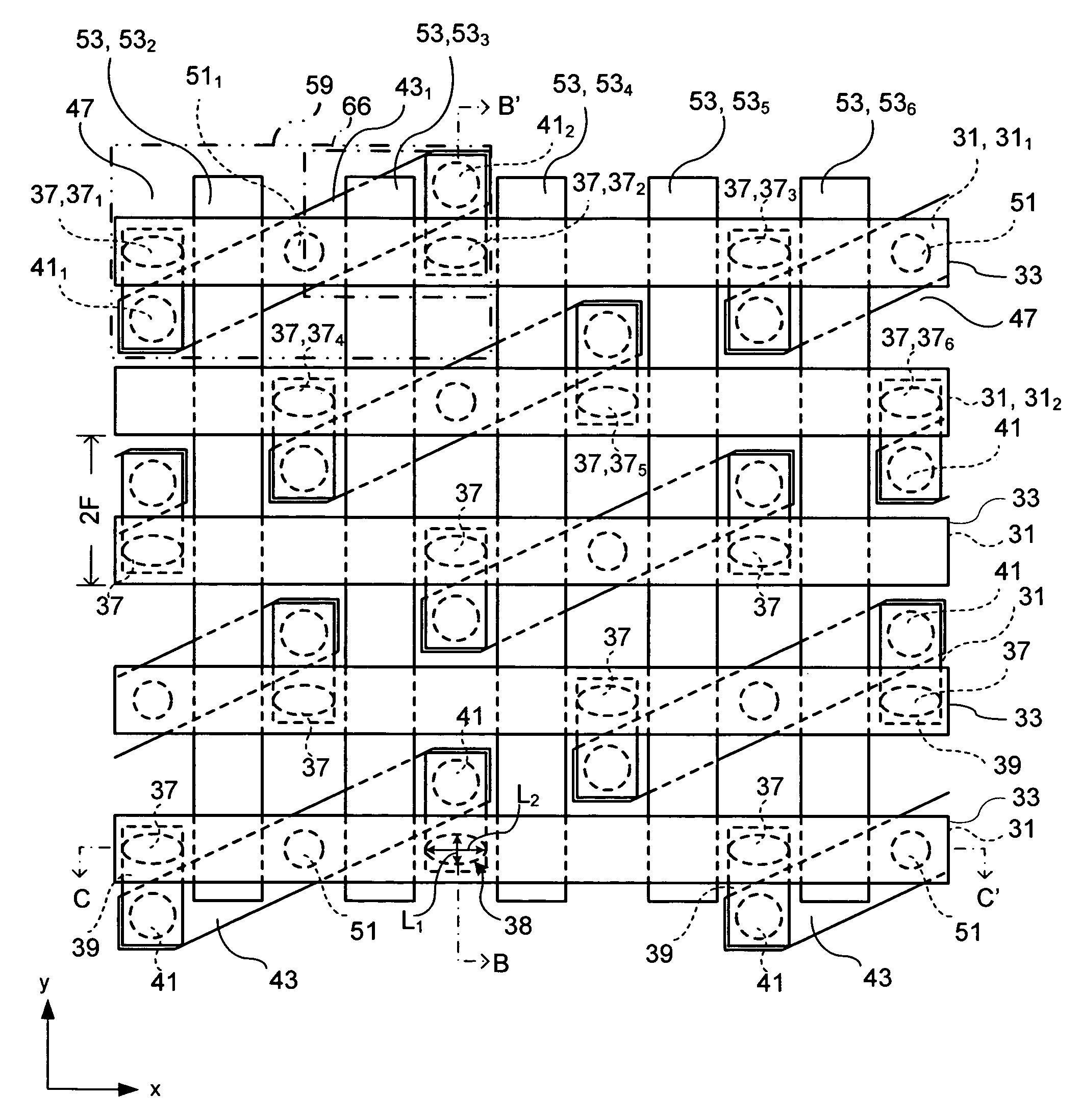
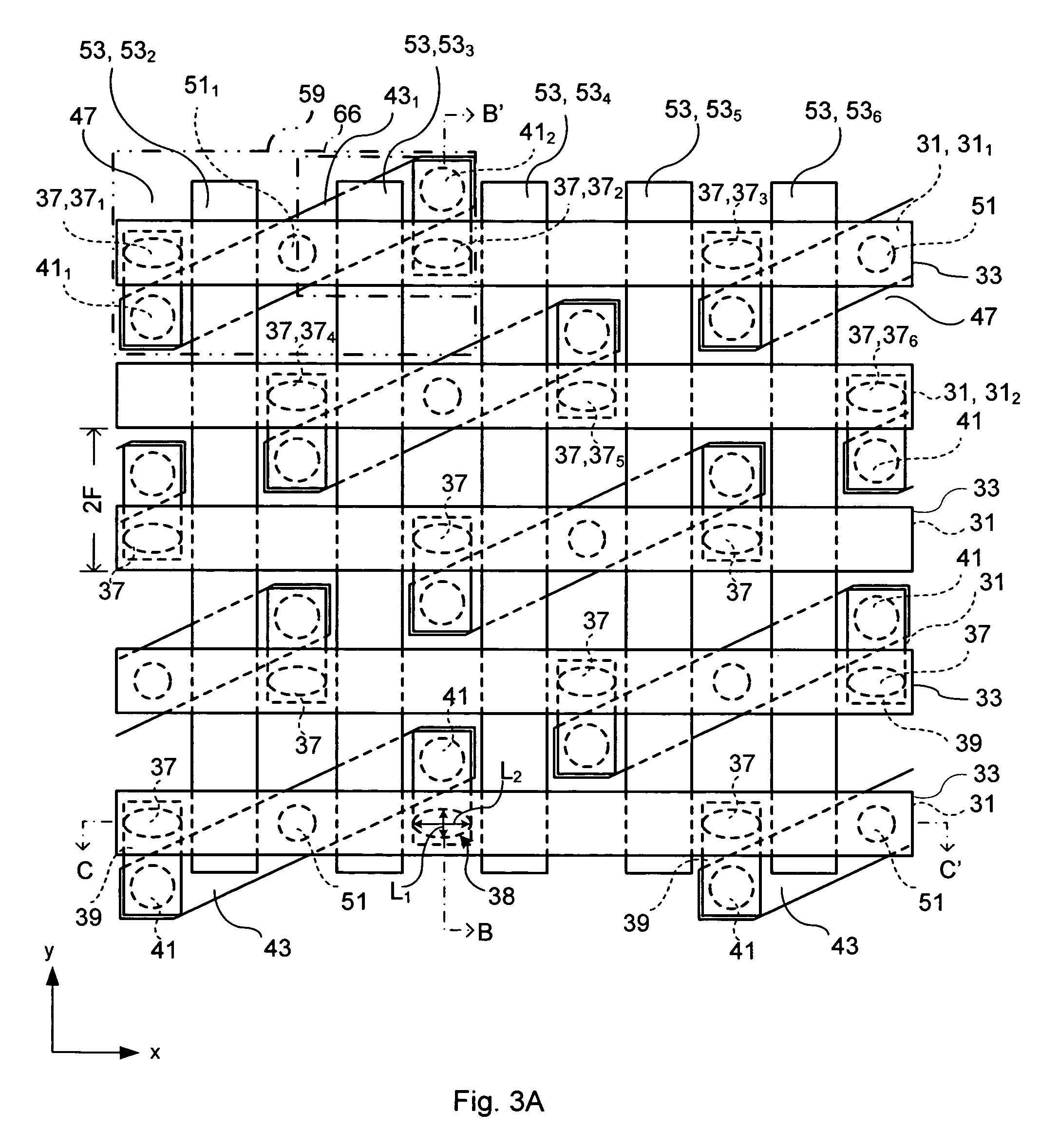
[0087]Referring to FIGS. 3A to 3D, a first memory array according to certain embodiments of the present invention is shown. The memory array is a magnetic random access memory (MRAM).

[0088]Referring in particular to FIG. 3A, the memory array is made up of a plurality of word lines 53, defining a first dimension of the array, in this example columns of the array, and a plurality of bit lines 31, overlying and perpendicular to the word lines 53, defining a second dimension of the array, in this example rows of the array.

[0089]A plurality of magnetic tunnel junctions (MTJs) 37 having stacked layers are connected to the underside of each bit line 31, in spaces between the word lines 53.

[0090]The bit lines 31 are arranged in a first direction, herein defined as the x-axis. The word lines 53 are arranged in a second direction, herein defined as the y-axis

[0091]Referring in particular to FIGS. 3B and 3C, a plurality of assist current lines 33 are arranged parallel to the x-axi...

second embodiment

Device Layout

[0192]Referring to FIGS. 12A to 12C, a second memory array according to certain embodiments of the present invention is shown. The memory array is an MRAM.

[0193]Referring in particular to FIG. 12A, a plurality of bit lines 201 are arranged in a first direction, herein defined as the x-axis. The bit lines 201 define a first dimension of the array, in this example, rows of the array. An assist current line 203 overlies each bit lines 201, and is electrically isolated from the respective bit line 201 by an insulating matrix 205.

[0194]A plurality of MTJs 207 are provided. The MTJs 207 have the same structure as the MTJs 37 described above with respect the first embodiment. The MTJs 207 are arranged with the magnetic easy axis parallel to the bit lines 201, i.e. parallel to the x-axis.

[0195]Referring in particular to FIG. 12B, Each MTJ 207 is connected to the underside of a bit line 201. Thus, the MTJs 207 are electrically isolated from the assist current lines 203.

[0196]Ref...


PUM

PropertyMeasurementUnit
thicknessaaaaaaaaaa
thicknessaaaaaaaaaa
widthaaaaaaaaaa

Abstract

A magnetic memory device comprises a magnetic tunnel junction (MTJ) connecting to a bit line to a sense line through an isolation transistor. The MTJ includes a ferromagnetic layer having a magnetic hard axis. An assist current line overlies the bit line and is insulated from the bit line. The MTJ is switchable between a first, relatively high resistance state and a second, relatively low resistance state. The assist current line applies a magnetic field along the magnetic hard axis in the ferromagnetic layer, independently of current flow through the MTJ for assisting switching of the MTJ between the first and second states.

Description

FIELD OF THE INVENTION[0001]The present invention relates to a magnetic memory device and in particular, although not exclusively, to a magnetic random access memory. The present invention relates also to a method of writing to a magnetic memory device.BACKGROUND ART[0002]The emergence of magnetic random access memory (MRAM) is a promising step for the development of both long-term and short-term data storage. MRAM has the benefit of being non-volatile, while having a lower energy consumption and faster read and write time than Flash memory. MRAM also has a lower energy consumption than the commonly used volatile memories dynamic RAM (DRAM) and static RAM (SRAM), with a read and write time faster than that of DRAM.[0003]A conventional MRAM cell comprises a magnetic element having a ferromagnetic free layer and a ferromagnetic pinned layer, separated by a non-magnetic layer. The pinned layer has a relatively high coercivity, so that its magnetisation remains fixed upon the applicatio...

Claims


Application Information

Patent Timeline
Patent Type & Authority Applications(United States)
IPC IPC(8): G11B5/33
CPCY10S977/935G11C11/16G11C11/15
Inventor ITO, KENCHITAKAHASHI, HIROMASAKAWAHARA, TAKAYUKITAKEMURA, RIICHIRODEVOLDER, THIBAULTCROZAT, PAULKIM, JOO-VONCHAPPERT, CLAUDE
Owner CENT NAT DE LA RECHERCHE SCI
Why Eureka
Try Eureka