Memory device with separate read and write gate voltage controls

a gate voltage control and memory device technology, applied in the direction of information storage, static storage, digital storage, etc., can solve the problems of weak cell failure or bit line sense amplifier malfunction, unwanted “read reverse-current” phenomenon,

Active Publication Date: 2008-02-14
SAMSUNG ELECTRONICS CO LTD
View PDF1 Cites 387 Cited by
  • Summary
  • Abstract
  • Description
  • Claims
  • Application Information

AI Technical Summary

Problems solved by technology

Memory devices having conventional chip architectures typically fall short of these goals, particularly as the requirements for density, power consumption and speed are repeatedly extended.
Various problems may arise due to the different supply voltages for the cell array and peripheral circuits, particularly in cases where a current-mode data sense amplifier having a load transistor is used.
For example, an unwanted “read reverse-current” phenomenon may occur during read operations, where current from a periphe...

Method used


Image

  • Memory device with separate read and write gate voltage controls
  • Memory device with separate read and write gate voltage controls
  • Memory device with separate read and write gate voltage controls

Examples


Embodiment Construction

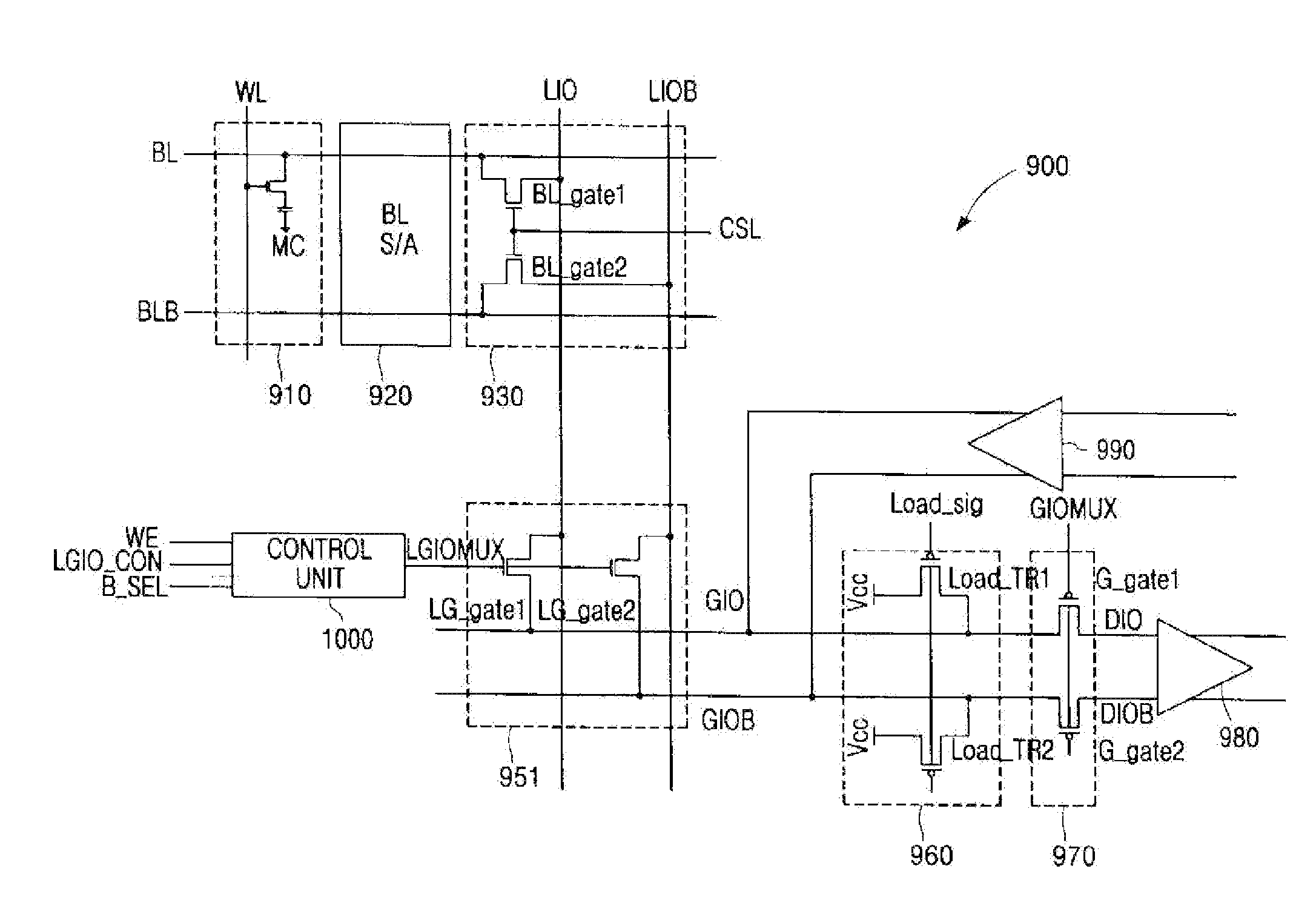
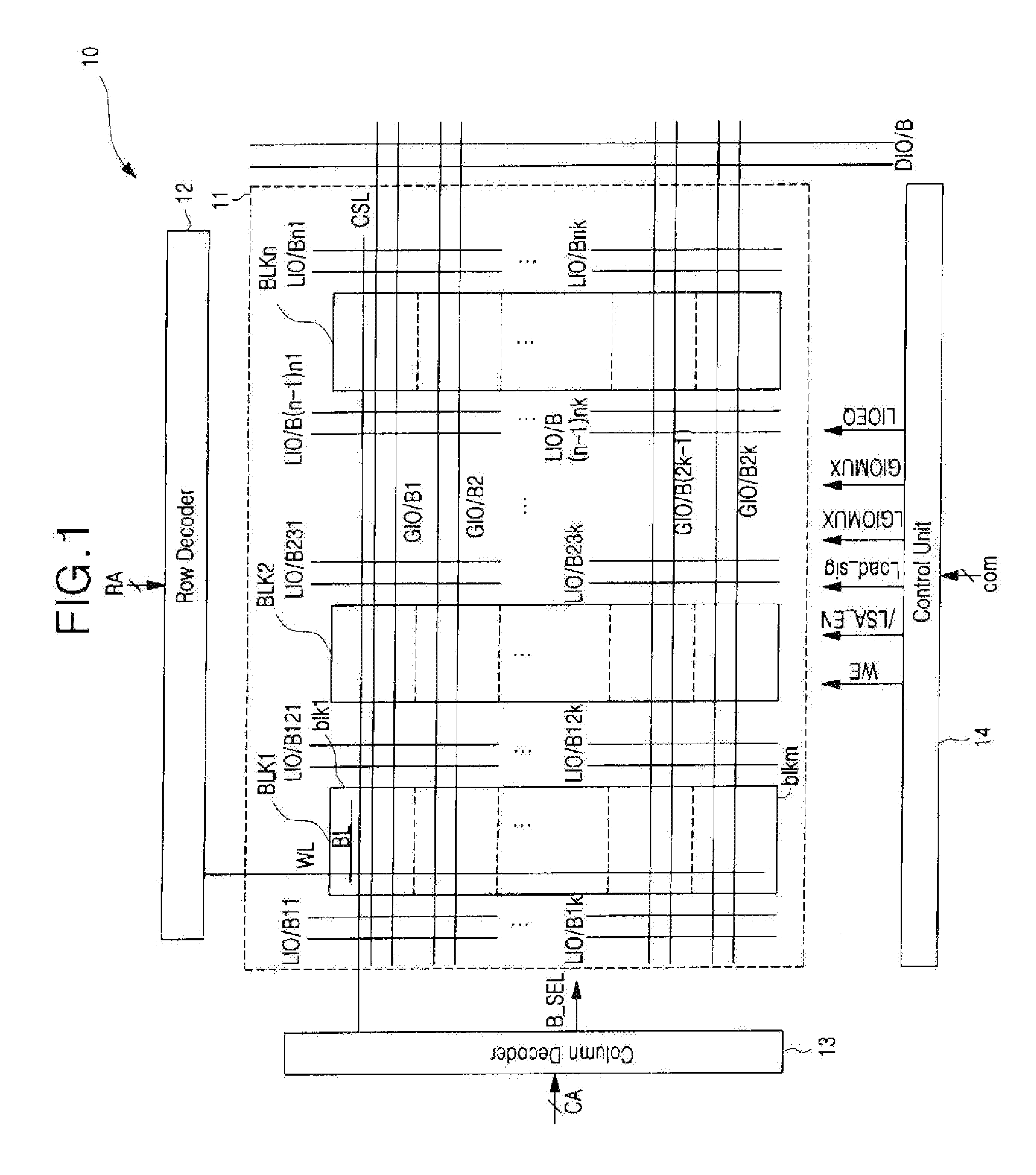
[0028]The present disclosure presents an apparatus and method for memory devices with separate read and write gate voltage controls. An exemplary embodiment uses two different gate voltages for a multiplexer (MUX) between Local I / O and Global I / O. Here, a lower gate voltage for “read” operations leads to higher resistance, and a higher gate voltage for “write” operations leads to lower resistance. A user selectable local sense amplifier (LSA) also can be employed. A mode register set (MRS) can be used to select (i.e., to enable) the local sense amplifier during read operation.

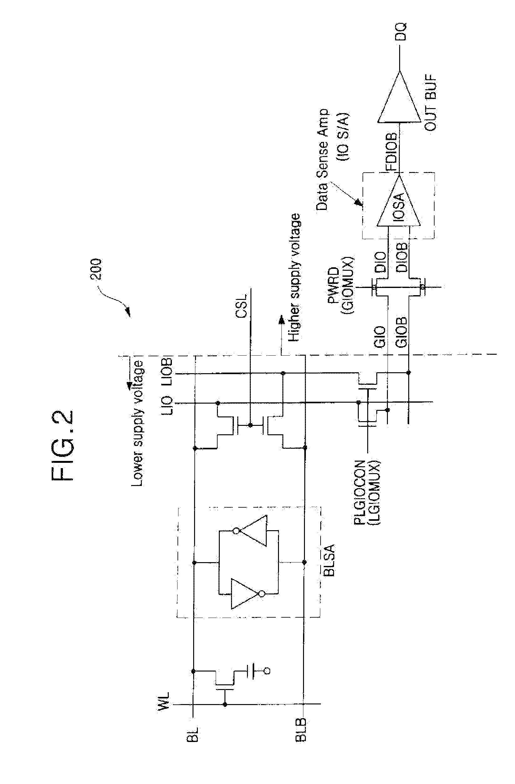
[0029]Turning to FIG. 2, a typical read path is indicated generally by the reference numeral 200. The read path 200 includes a word line (WL) in signal communication with bit lines (BL / BLB). The BL / BLB are in signal communication with a bit line sense amplifier (BLSA). The BL / BLB are in signal communication with local I / O lines(LIO / LIOB) via column select transistors responding a column select line (CSL) signal...


PUM


Abstract

A circuit and method are provided for controlling the gate voltage of a transistor acting between local and global input/output lines of a memory device, the circuit including a local input/output line, a local from/to global input/output multiplexer in signal communication with the local input/output line, a global input/output line in signal communication with the local from/to global input/output multiplexer, and a local from/to global input/output controller having an input node and an output node, the input node disposed for receiving a signal indicative of an input or output operation, and the output node in signal communication with a gate of the local from/to global input/output multiplexer for providing a gate signal of a first or second level in the presence of the output operation, and a gate signal of a third level in the presence of the input operation.

Description

CROSS-REFERENCE TO RELATED APPLICATION[0001]This application claims foreign priority under 35 U.S.C. 119 to Korean Patent Application No. 10-2006-0034711, filed on Apr. 17, 2006 in the Korean Intellectual Property Office, the disclosure of which is incorporated by reference herein in its entirety.BACKGROUND OF THE INVENTION[0002]It is generally desirable to achieve high density, low power consumption, and high-speed operation all in the same memory device. Memory devices having conventional chip architectures typically fall short of these goals, particularly as the requirements for density, power consumption and speed are repeatedly extended.[0003]As shown in FIG. 1, a memory device with conventional chip architecture is indicated generally by the reference numeral 10. The memory device 10 includes a plurality of banks like the bank 11 having a plurality of memory cell array blocks BLK1 through BLKn, a plurality of sub-memory cell array blocks blk1 through blkm, a word line WL and a...

Claims


Application Information

Patent Timeline
IPC IPC(8): G11C7/10
CPCG11C7/1051G11C7/1069G11C2207/002G11C11/4093G11C11/4097G11C7/18G11C7/10
Inventor KIM, KYOUNG HOJANG, SEONG JIN
Owner SAMSUNG ELECTRONICS CO LTD
Why Eureka
Try Eureka