Self-timing circuit with programmable delay and programmable accelerator circuits

a self-timing circuit and accelerator technology, applied in the field of self-timing circuits, can solve the problems of unnecessarily long access time of memory, insufficient magnitude of differential voltage, and inability to output erroneous data by sense amplifiers, etc., and achieve the effect of fast access time and slow access tim

Active Publication Date: 2008-02-14
QUALCOMM INC
View PDF3 Cites 48 Cited by
  • Summary
  • Abstract
  • Description
  • Claims
  • Application Information

AI Technical Summary

Benefits of technology

[0012]In one example, the circuitry for programmably changing the speed of the timing loop includes a programmable delay circuit and a programmable accelerator circuit. Control signals are supplied to the programmable delay circuit to control the amount of propagation delay introduced into the signal path of the self-timing loop by the programmable delay circuit. Control signals are supplied to the programmable accelerator circuit to control the degree to which the accelerator circuit accelerates the self-timing loop. The control signals supplied to the programmable delay circuit and the programmable accelerator circuit can be set under software control or can be hardwired depending on the implementation. In one novel method, the programmable delay and accelerator circuits are usable to change the speed of the self-timing loop to achieve a desired yield to memory access speed tradeoff. Memories of a single design can be graded and / or separated into two groups by appropriate control of the self-timing circuit: a first group can be made to have faster access times, whereas a second group can be made to have slower access times. Flexibility of the timing loop allows a memory to be designed before memory access timing characteristics are fixed or are known. Where a silicon compiler program is used to fashion different formats and configurations of memories, the self-timing circuit is incorporated into each memory design so that timing of the self-timed control signals can be adjusted as appropriate for the particular design and memory array to be accessed.

Problems solved by technology

If the time between the edge of the clock signal and the sense amplifier enable signal is too short, then the magnitude of the differential voltages may be too small and the sense amplifiers may output erroneous data.
On the other hand, if the time between the edge of the clock signal and the sense amplifier enable signal is longer than necessary, then the access time of the memory is lengthened unnecessarily.
If, however, the address latch were made transparent for the next memory cycle too early with respect to disabling of the sense amplifiers, then the sense amplifiers may erroneously change the values they are outputting at the end of the prior memory read operation.

Method used


Image

  • Self-timing circuit with programmable delay and programmable accelerator circuits
  • Self-timing circuit with programmable delay and programmable accelerator circuits
  • Self-timing circuit with programmable delay and programmable accelerator circuits

Examples


Embodiment Construction

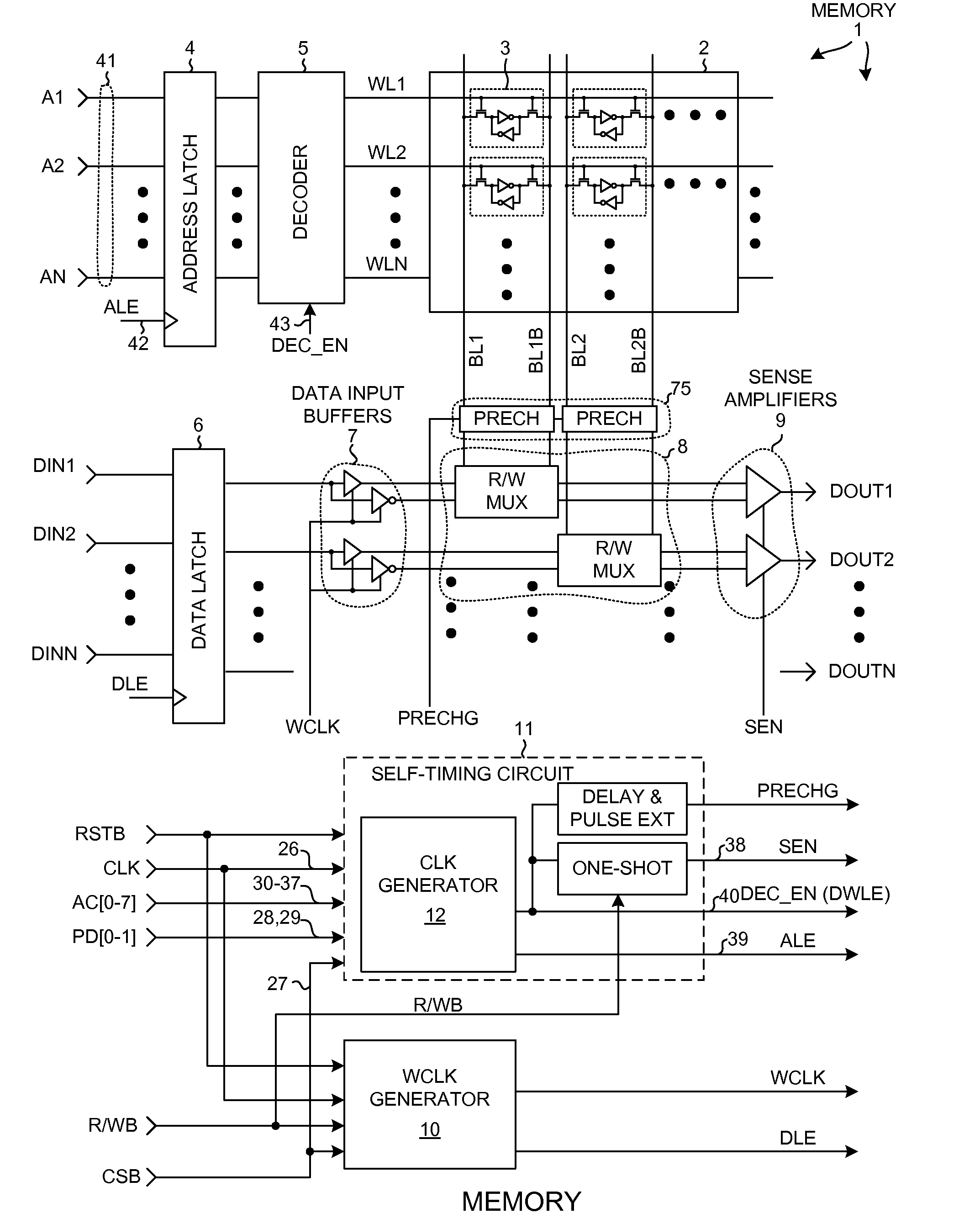
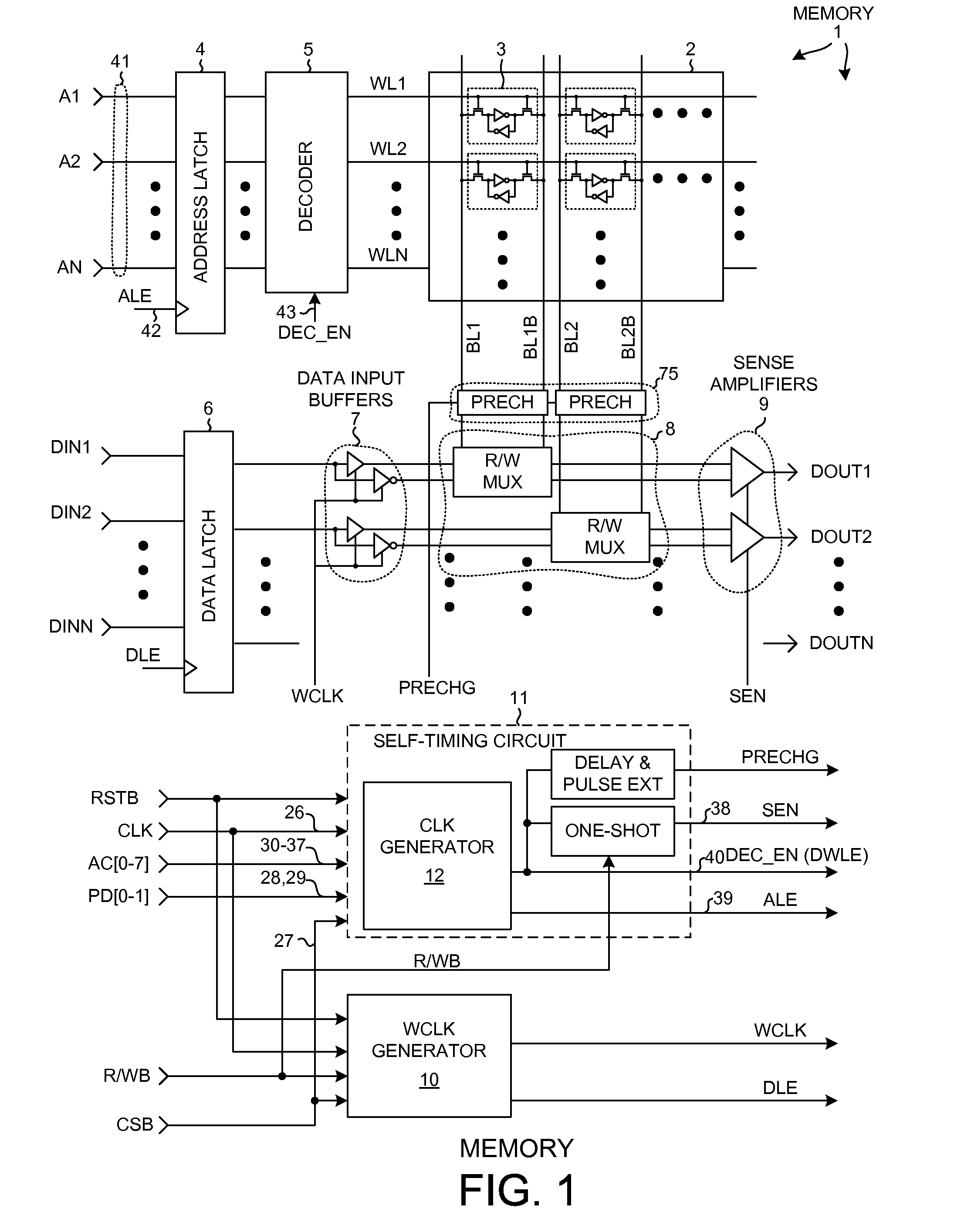
[0017]FIG. 1 is a simplified diagram of a semiconductor memory integrated circuit device 1. Memory device 1 is a static random access memory (SRAM). Memory device 1 includes an array 2 of bit cells 3 that are arranged in rows and columns. Each row of bit cells has an associated horizontally extending word line. The word lines are designated WL1 through WLN in the figure. Each column of bit cells has an associated pair of vertically extending bit lines. In the diagram, the leftmost pair of bit lines is designed BL1 and BL1B and the next leftmost pair of bit lines is designated BL2 and BL2B. As illustrated, each bit cell is a six-transistor cell and involves a cross-coupled pair of inverters and a pair of access transistors. Memory device 1 also includes an address latch 4, a row decoder 5, a data input latch 6, data input buffers 7, read / write multiplexers 8, sense amplifiers 9, precharge circuits 75, a write clock generator circuit 10, and a self-timing circuit 11.

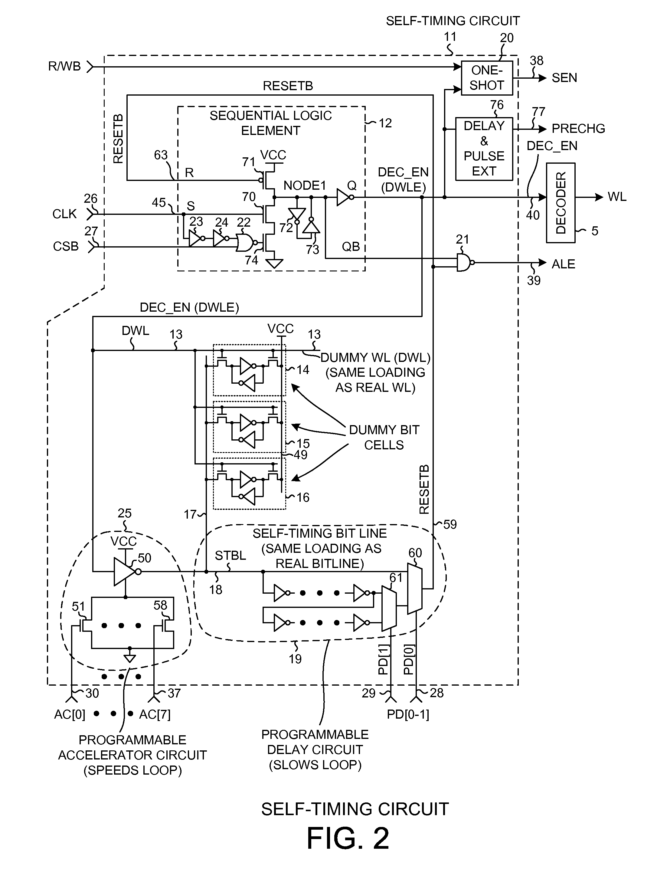
[0018]FIG. 2 is a ...


PUM


Abstract

A memory has a novel self-timing circuit that generates internal memory control signals. Control signals may include an address latch enable signal, a decoder enable signal, and a sense amplifier enable signal. The circuit has a timing loop whose timing mimics the timing of an access of the real memory. The timing loop includes dummy bit cells of identical construction to bit cells in the real array being accessed, a programmable delay circuit, and a programmable accelerator circuit. The dummy bit cells cause the timing of the control signals to track speed changes in the memory array being accessed. The programmable delay and accelerator circuits are usable to slow or speed the timing loop. The programmable delay and accelerator circuits are usable to achieve a desired yield to memory access speed tradeoff. Flexibility of the timing loop allows a memory to be designed before memory access timing characteristics are fixed.

Description

CROSS-REFERENCE TO RELATED APPLICATION[0001]This application claims the benefit under 35 U.S.C. §119 of Provisional Application Ser. No. 60 / 836,779, filed Aug. 9, 2006, said provisional application is incorporated herein by reference.BACKGROUND INFORMATION[0002]1. Technical Field[0003]The disclosed embodiments relate to self-timing circuits that generate internal memory control signals in semiconductor memory devices.[0004]2. Background Information[0005]One conventional type of semiconductor memory device is a static random access memory (SRAM) that involves an array of bit cells organized in rows and columns. Each row of bit cells has an associated word line. Each column of bit cells has an associated pair of bit lines. Each pair of bit lines is coupled to a sense amplifier. If the sense amplifier detects a positive differential voltage between its pair of bit lines, then the sense amplifier outputs a first digital logic value. If, on the other hand, the sense amplifier detects a n...

Claims


Application Information

Patent Timeline
Patent Type & Authority Applications(United States)
IPC IPC(8): G11C7/00
CPCG11C7/14G11C7/22G11C7/222G11C29/023G11C11/417G11C29/02G11C11/41
Inventor CHEN, ZHIQINJUNG, CHANG HO
Owner QUALCOMM INC
Why Eureka
Try Eureka