Apparatus and method for polishing semiconductor wafers

a technology of semiconductor wafers and polishing tools, applied in the direction of grinding machine components, manufacturing tools, lapping machines, etc., can solve the problem of greater operation cos

Inactive Publication Date: 2008-02-14
KOMICO TECH
View PDF9 Cites 11 Cited by
  • Summary
  • Abstract
  • Description
  • Claims
  • Application Information

AI Technical Summary

Problems solved by technology

However, the footprint of a CMP equipment must also be considered since a CMP equipment with a large footp

Method used


Image

  • Apparatus and method for polishing semiconductor wafers
  • Apparatus and method for polishing semiconductor wafers
  • Apparatus and method for polishing semiconductor wafers

Examples


Embodiment Construction

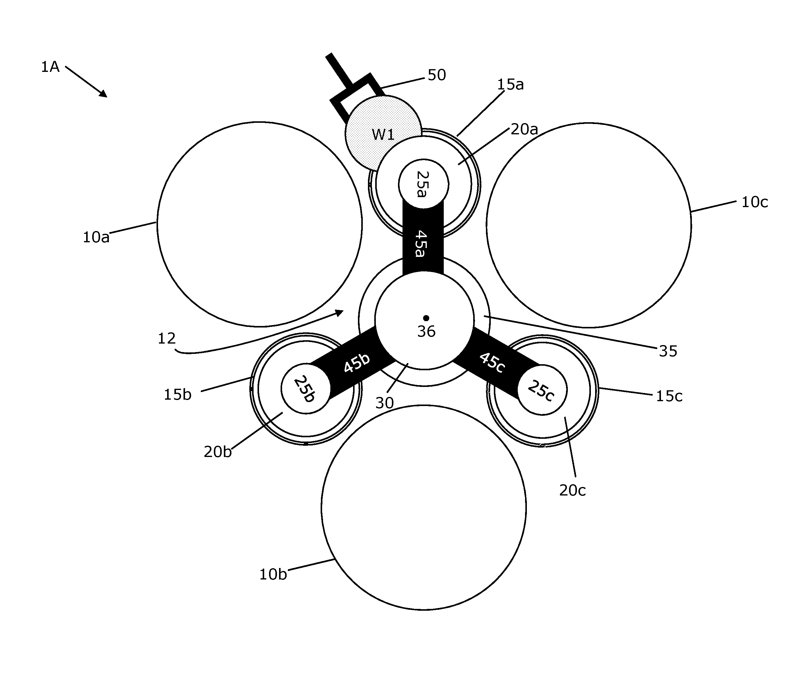
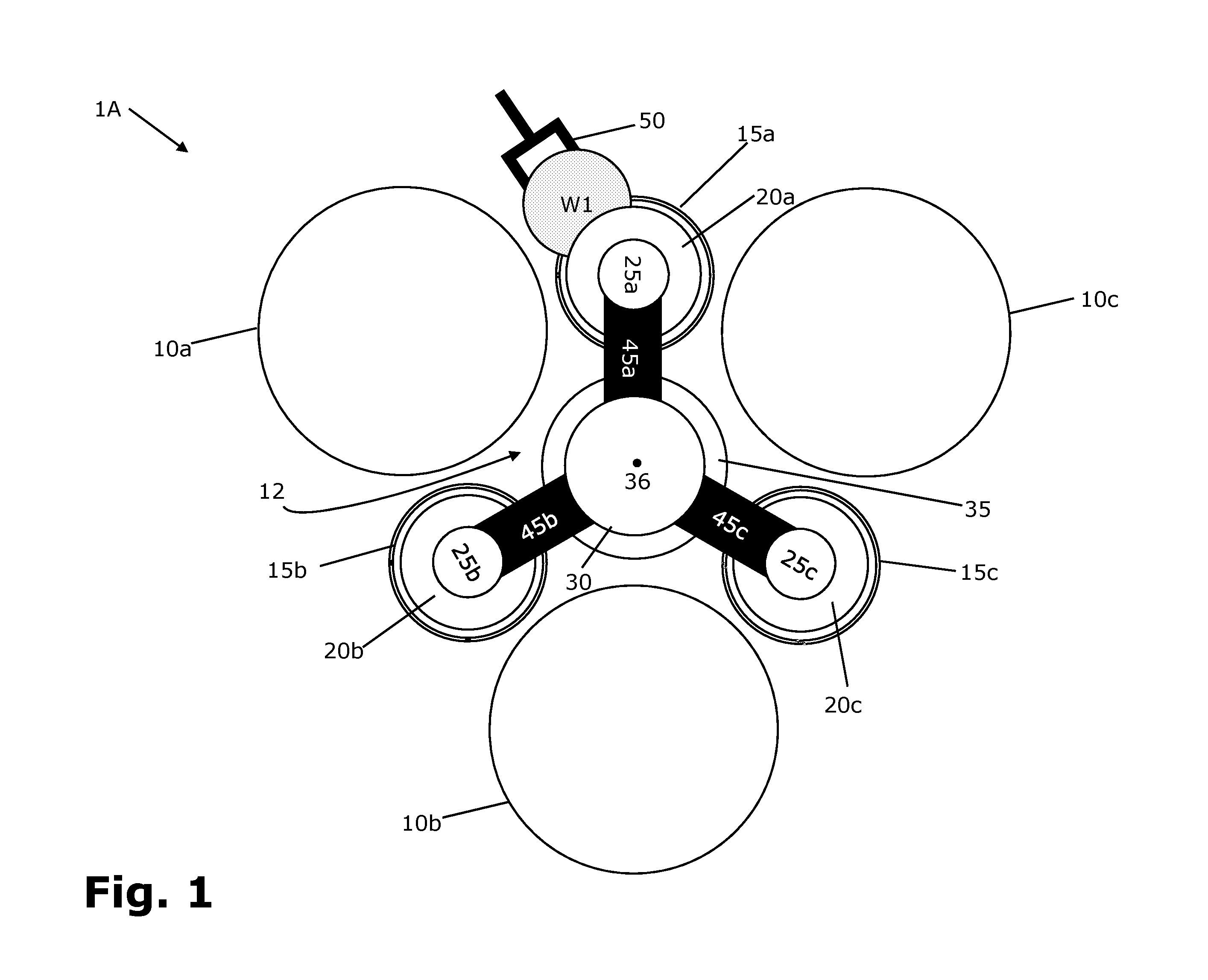
[0047]With reference to FIGS. 1-3, a polishing apparatus 1A according to an embodiment of the invention is described. The polishing apparatus 1A comprises three polishing surfaces 10a-10c, three polishing heads 20a-20c and three wafer load-unload stations 15a-15c. The polishing apparatus 1A can further comprise a wafer transfer device 50. The polishing apparatus 1A is capable of sequentially processing multiple semiconductor wafers, as described in more detail below.

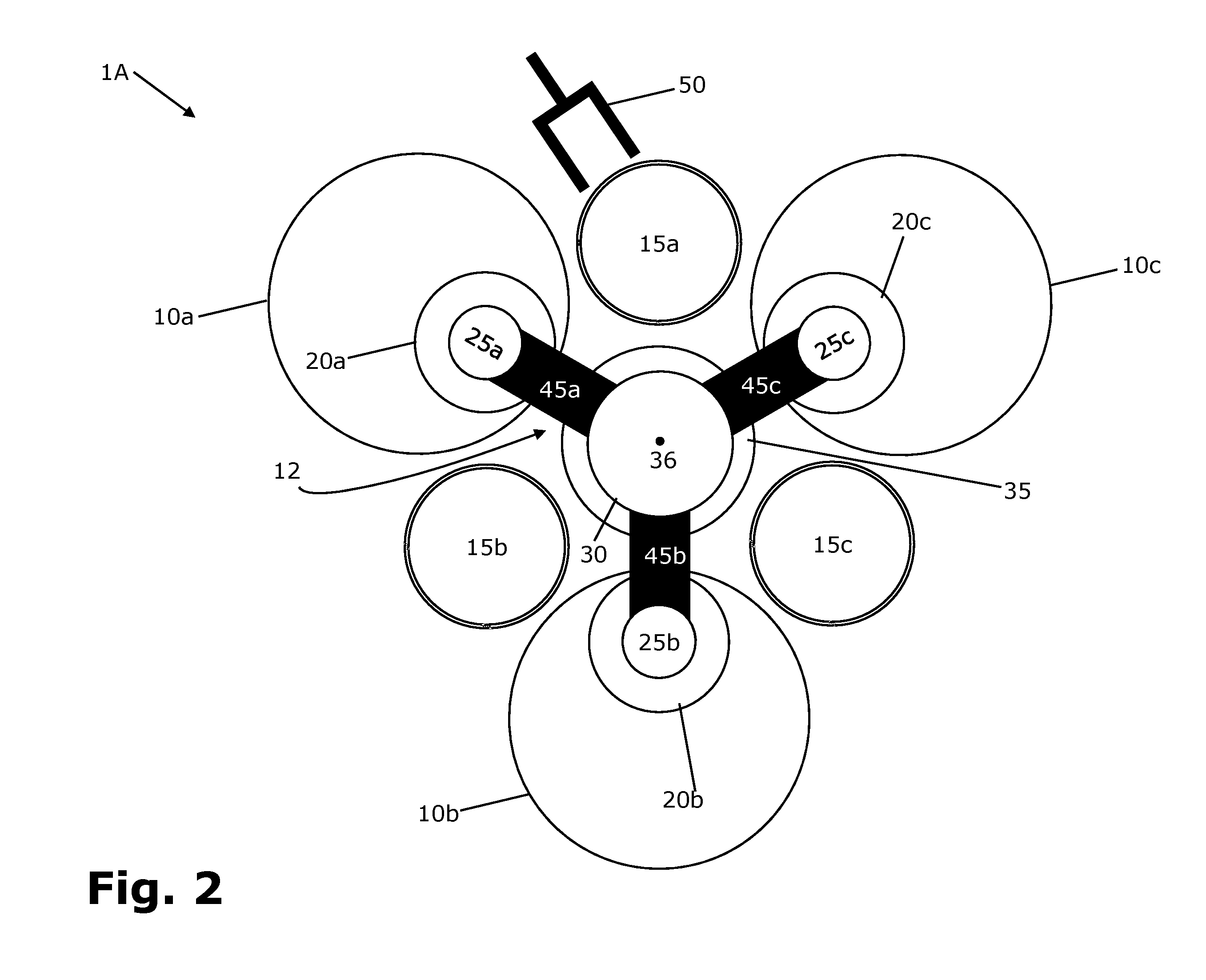
[0048]FIG. 1 shows the polishing apparatus 1A when the first, second and third polishing heads 20a-20c are positioned over the first, second and third wafer load-unload stations 15a-15c, respectively. FIG. 2 shows the polishing apparatus 1A when the first, second and third polishing heads 20a-20c are positioned over the first, second and third polishing surfaces 10a-10c, respectively. FIG. 3 shows the polishing apparatus 1A when the first, second and third polishing heads 20a-20c are positioned over the second, third and...


PUM


Abstract

An apparatus and method for polishing semiconductor wafers uses multiple polishing surfaces, multiple polishing heads and multiple wafer stations to sequentially polish the semiconductor wafers. The wafer stations includes at least one wafer load-unload station to transfer the semiconductor wafers between the wafer load-unload station and the polishing heads.

Description

CROSS REFERENCE TO RELATED APPLICATION[0001]This application is entitled to the benefit of U.S. Provisional Patent Application Ser. Nos. 60 / 836,278, filed on Aug. 8, 2006, 60 / 837,276, filed on Aug. 10, 2006, 60 / 840,192, filed on Aug. 25, 2006, 60 / 840,143, filed on Aug. 26, 2006, and 60 / 844,150, filed on Sep. 12, 2006, which are all incorporated herein by reference.FIELD OF THE INVENTION[0002]The invention relates generally to semiconductor processing equipments, and more particularly to an apparatus and method for polishing semiconductor wafers.BACKGROUND OF THE INVENTION[0003]Local and global planarization of semiconductor wafers becomes increasingly important as more metal layers and interlayer dielectric layers are stacked on the wafers. A preferred method to planarize semiconductor wafers is the chemical mechanical polishing (CMP) method, where a surface of a semiconductor wafer is polished using a slurry solution supplied between the wafer and a polishing pad. The CMP method is...

Claims


Application Information

Patent Timeline
IPC IPC(8): B24B51/00
CPCB24B37/345
Inventor JEONG, IN-KWON
Owner KOMICO TECH
Why Eureka
Try Eureka