
Method for Forming Carbonaceous Material Protrusion and Carbonaceous Material Protrusion
a carbonaceous material and projection technology, applied in the manufacture of electronic devices, chemical vapor deposition coatings, record information storage, etc., can solve the problems of uneven light propagation, low projection angle, and inability to efficiently emit electrons from the nea surface, so as to improve the uniformity of projection height, improve the reproducibility of device fabrication, and improve the effect of current density
- Summary
- Abstract
- Description
- Claims
- Application Information
AI Technical Summary
Benefits of technology
Problems solved by technology
Method used
Image

Examples
example 1
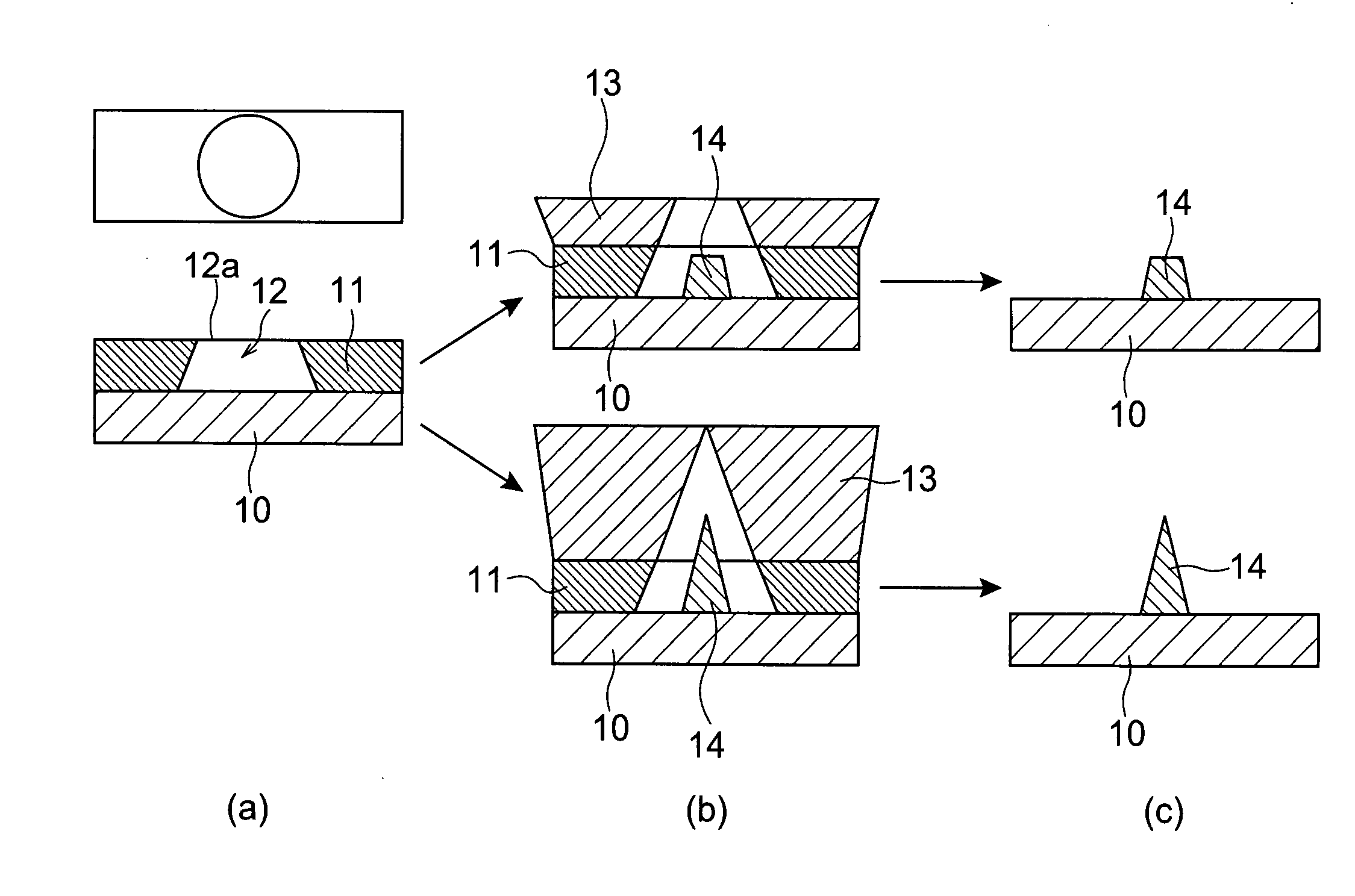
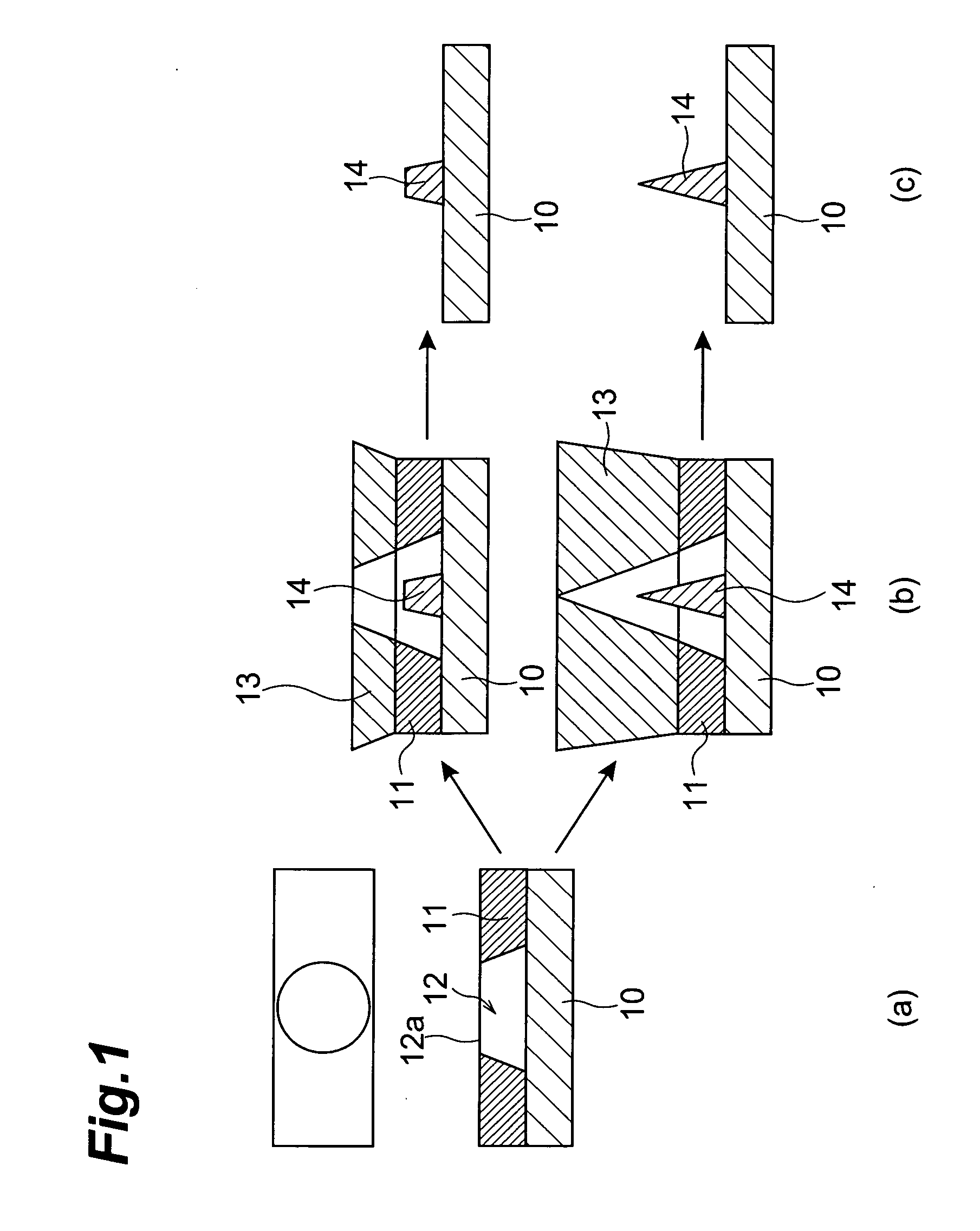
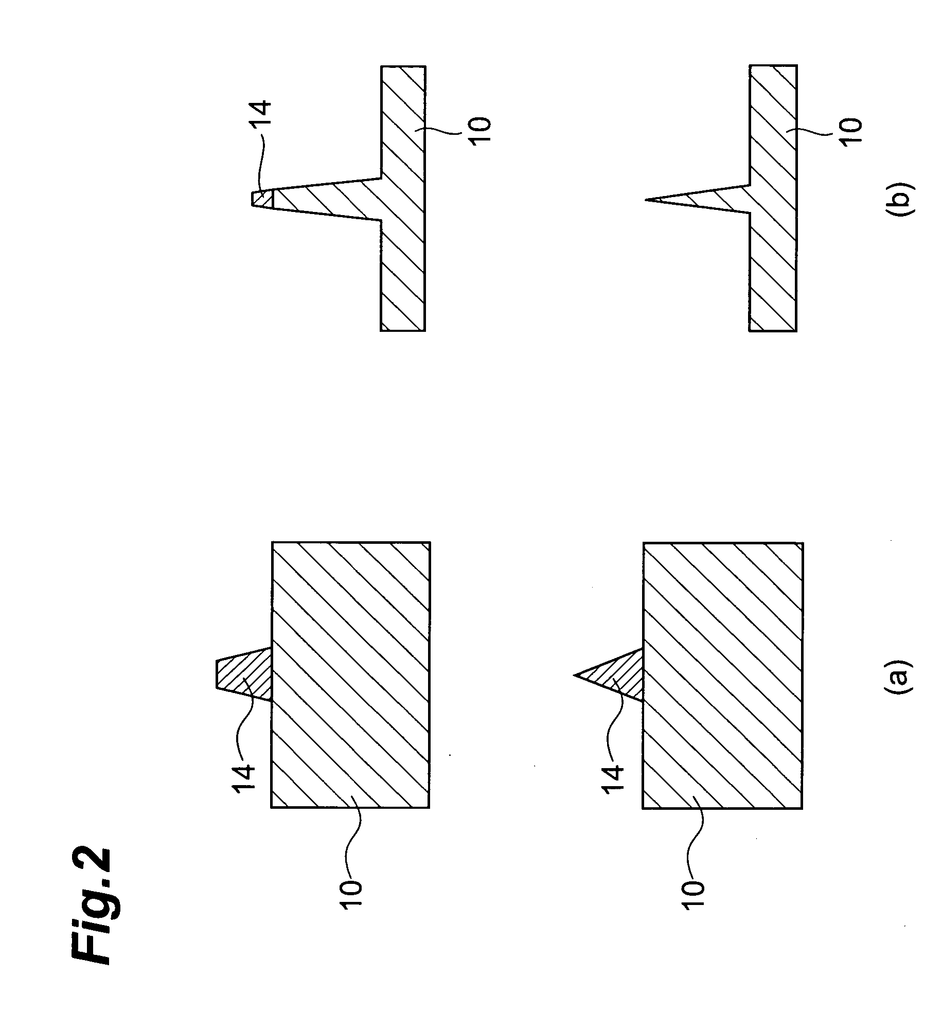
[0077]A high-pressure-synthesized single-crystal diamond substrate (100) and a CVD polycrystalline diamond wafer substrate were planarized to not more than several nm by polishing to prepare substrates, the prepared substrates were coated with resist for electron beam lithography, electron beam exposure was conducted, and holes of inversely tapered shape were formed (cf. part (a) of FIG. 1). Then, a metal film of one of Au, Mo, Pt, and Al was deposited on them, and the resist was removed thereafter to lift off the metal film (cf. part (c) of FIG. 1). Diamond etching was performed using the mask, whereby extremely acute diamond projections were formed as shown in part (a) of FIG. 4 and in part (b) of FIG. 4. Part (a) of FIG. 4 shows a projection shape formed by use of a circular truncated cone mask or a projection shape formed by use of a circular cone mask and by stopping the etching before complete removal of the mask. Part (b) of FIG. 4 shows a projection of a pointed shape formed...
example 2
[0080]A high-pressure-synthesized single-crystal diamond substrate (100), a CVD polycrystalline diamond wafer substrate, and a SiC substrate were planarized to not more than several nm by polishing to prepare substrates. Each of these prepared substrates was implanted with ions of inert gas or nitrogen to prepare a sample. Some of these samples were treated by high-temperature anneal (1500° C. or 1800° C.) in vacuum, and the rest of these samples and samples not subjected to the ion implantation were processed at high temperature. On a surface of each of these samples, a black layer of electrically conductivity, which may be assumed to be graphite, was formed. A patterned mask of a projection shape was formed on the samples by the same method as in Example 1. The carbonaceous material was etched using them as masks, whereby extremely acute projections of the carbonaceous material were formed as shown in part (a) of FIG. 4 and in part (b) of FIG. 4. The carbonaceous material from the...
example 3
[0081]A high-pressure-synthesized single-crystal diamond substrate (100) and a CVD polycrystalline diamond wafer substrate were planarized to not more than several nm by polishing to prepare substrates, they were coated with resist for electron beam lithography, electron beam exposure was conducted, and holes of inversely tapered shape were formed (cf. part (a) of FIG. 1). A SiOx film was deposited thereon with a source material of SiO2 by the EB evaporation, the resist was removed thereafter, and the SiOx film was lifted off (cf. part (c) of FIG. 1). The composition of the SiOx film was close to SiO2 where a small amount of oxygen gas was introduced into the SiOx film. Where it was processed in inert gas or in high vacuum, the oxygen content was small in the film. The compositions are presented in FIG. 7. When diamond was etched using this mask, diamond columns with an extremely acute tip were formed. It was demonstrated that the diamond projections were formed using the mask of su...
PUM
| Property | Measurement | Unit |
|---|---|---|
| diameter | aaaaa | aaaaa |
| apex angle | aaaaa | aaaaa |
| diameter | aaaaa | aaaaa |
Abstract
Description
Claims
Application Information