Method of forming surface irregularities and method of manufacturing gallium nitride-based light emitting diode

Active Publication Date: 2008-02-21
SAMSUNG ELECTRONICS CO LTD
View PDF4 Cites 14 Cited by
  • Summary
  • Abstract
  • Description
  • Claims
  • Application Information

AI Technical Summary

Benefits of technology

[0019]An advantage of the present invention is that it provides a method of forming surface irregularities, which can form standardized surface irregularities on a GaN substrate by using a wet-etching process where an occurrence rate of defects is low.
[0020]Another advantage of the invention is that it provides a method of manufacturing a GaN-based LED which has standardized surface irregularities while a light-emission surface composed of a GaN substrate has a low occurrence rate of defects.
[0021]Additional aspect and advantages of the present general inventive concept will be set forth in part in the description which follows and, in part, will be obvious from the description, or may be learned by practice of the general inventive concept.
[0022]According to an aspect of the invention, a method of forming surface irregularities comprises preparing a GaN substrate; forming a mask on a surface of the GaN substrate,

Problems solved by technology

Generally, a GaN-based semiconductor LED is grown on a sapphire substrate, but the sapphire substrate is a rigid nonconductor and has poor thermal conductivity.
Therefore, there is a limitation in reducing the manufacturing costs by decreasing the size of a GaN-based sem

Method used


Image

  • Method of forming surface irregularities and method of manufacturing gallium nitride-based light emitting diode
  • Method of forming surface irregularities and method of manufacturing gallium nitride-based light emitting diode
  • Method of forming surface irregularities and method of manufacturing gallium nitride-based light emitting diode

Examples


Embodiment Construction

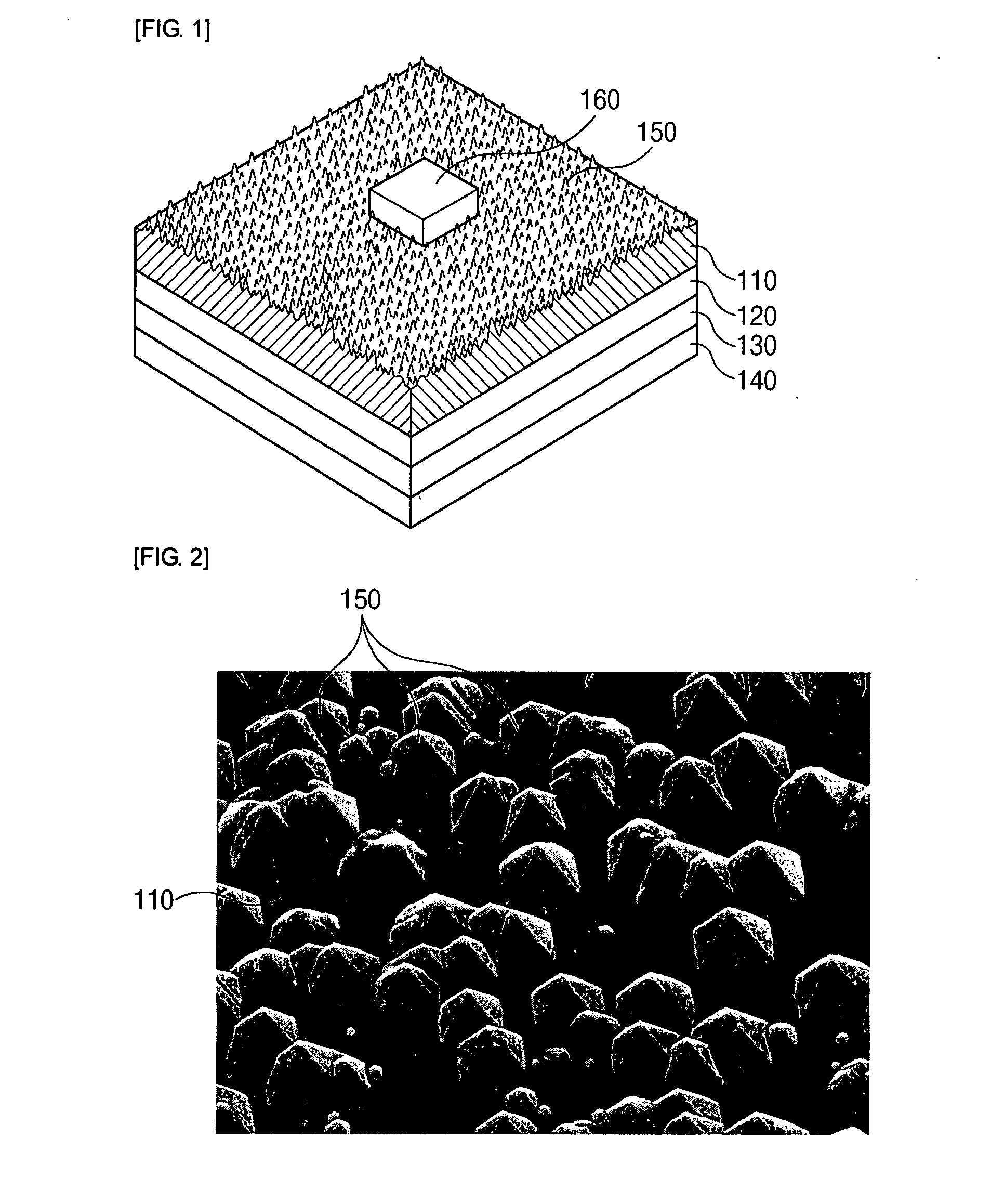
[0040]Reference will now be made in detail to the embodiments of the present general inventive concept, examples of which are illustrated in the accompanying drawings, wherein like reference numerals refer to like elements throughout. The embodiments are described below in order to explain the present general inventive concept by referring to the figures. In the drawings, the thicknesses of layers and regions are exaggerated for clarity.

[0041]Hereinafter, embodiments of the present invention will be described in detail with reference to the accompanying drawings.

[0042]Method of Forming Surface Irregularities

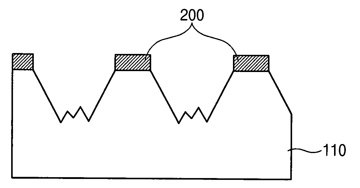
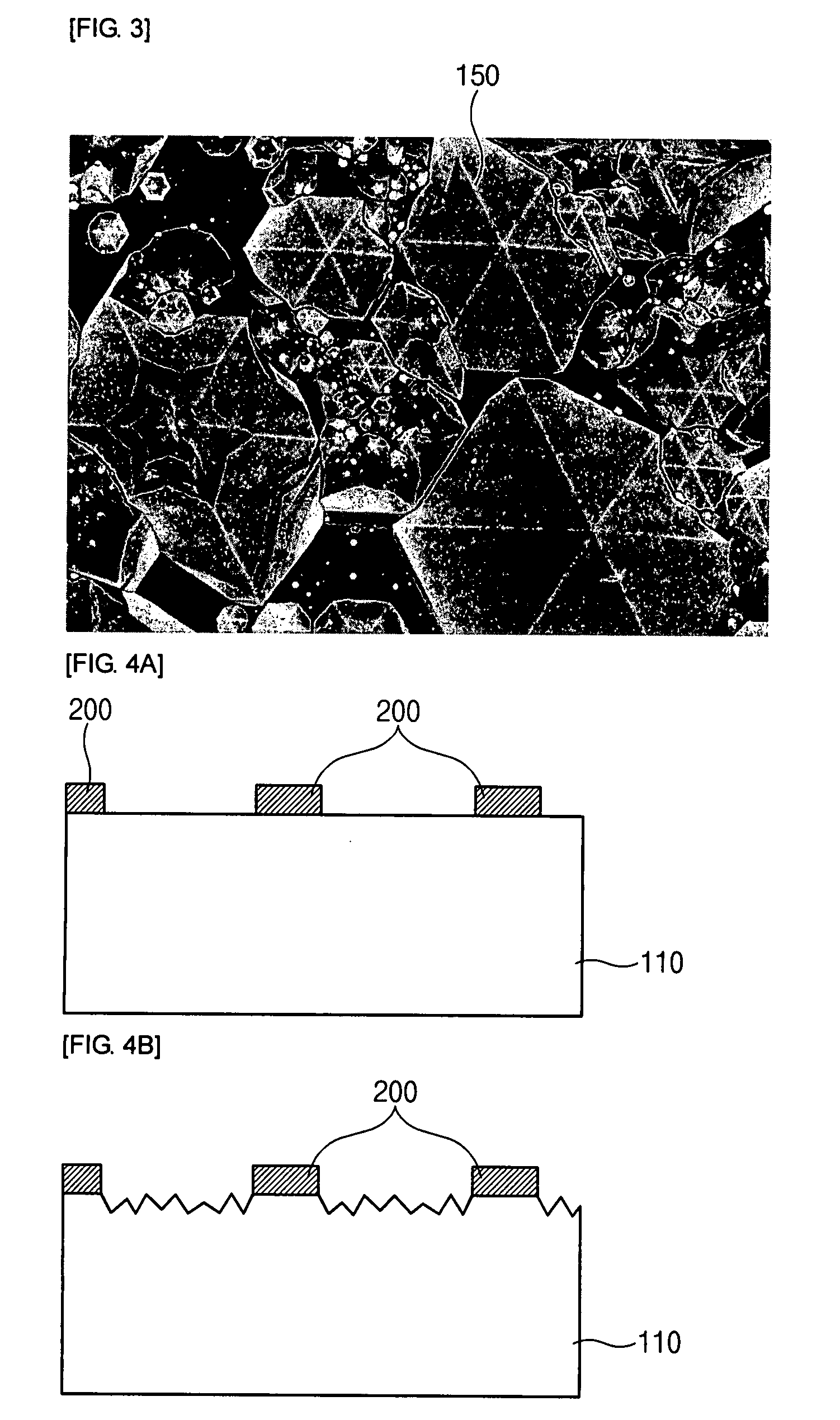
[0043]Referring to FIGS. 4A to 4D, 5, and 6, a method of forming surface irregularities according to an embodiment of the invention will be described in detail.

[0044]FIGS. 4A to 4D are sectional views sequentially showing a method of forming surface irregularities according to an embodiment of the invention, FIG. 5 is a photograph showing the cross-section of surface irregulariti...


PUM


Abstract

A method of forming surface irregularities comprises preparing a GaN substrate; forming a mask on a surface of the GaN substrate, the mask defining a surface-irregularity formation region; and wet-etching portions of the surface of the GaN substrate by using the mask as an etching mask. The wet-etching of the GaN substrate is performed until the end of one surface of the GaN substrate to be formed by the wet-etching using the mask meets the end of another surface of the GaN substrate to be formed by the wet-etching using the mask, the another surface being adjacent to the one surface.

Description

CROSS-REFERENCE TO RELATED APPLICATIONS[0001]This application claims the benefit of Korean Patent Application No. 10-2006-0077677 filed with the Korean Intellectual Property Office on Aug. 17, 2006, the disclosure of which is incorporated herein by reference.BACKGROUND OF THE INVENTION[0002]1. Field of the Invention[0003]The present invention relates to a method of forming surface irregularities and a method of manufacturing a gallium nitride-based light emitting diode (hereinafter, referred to as a GaN-based LED), which can enhance light extraction efficiency of a vertical GaN-based LED using a GaN substrate.[0004]2. Description of the Related Art[0005]Generally, a GaN-based semiconductor LED is grown on a sapphire substrate, but the sapphire substrate is a rigid nonconductor and has poor thermal conductivity. Therefore, there is a limitation in reducing the manufacturing costs by decreasing the size of a GaN-based semiconductor LED, or improving the optical power and chip characte...

Claims


Application Information

Patent Timeline
IPC IPC(8): H01L21/00H01L33/06H01L33/10H01L33/22H01L33/32
CPCH01L33/32H01L33/22
Inventor CHOI, PUN JAEKOIKE, MASAYOSHIHO, LEE JONG
Owner SAMSUNG ELECTRONICS CO LTD
Why Eureka
Try Eureka