This helps you quickly interpret patents by identifying the three key elements:
Problems solved by technology
Method used
Benefits of technology
Benefits of technology
[0003] It is an object of the present invention to provide a semiconductor device in which data can be written except when manufacturing a chip and that counterfeits can be prevented. Moreover, it is another object of the invention to provide an inexpensive semiconductor device including a memory element having a simple structure.
[0018] According to the invention, a semiconductor device in which data can be written (written once, read many) except when manufacturing a memory circuit and that counterfeits can be prevented. In addition, a semiconductor device according to the invention can operate at high speed since a transistor using a single crystal semiconductor layer having favorable mobility and response speed as a channel portion is included. Further, according to the invention, a memory element having a simple structure can be formed; therefore, a semiconductor device having an inexpensive and highly integrated memory element can be provided.
Problems solved by technology
In these memory elements, writing (writing once, reading many) data cannot be conducted except when manufacturing the memory element; therefore, the memory elements are inconvenient.
Method used
Image
Click on the blue label to locate the original text in one second.
Reading with bidirectional positioning of images and text.
Examples
embodiment mode 1
[0045] In this embodiment mode, one example of the structure of a semiconductor device according to the present invention is explained with reference to FIGS. 1 to 3.
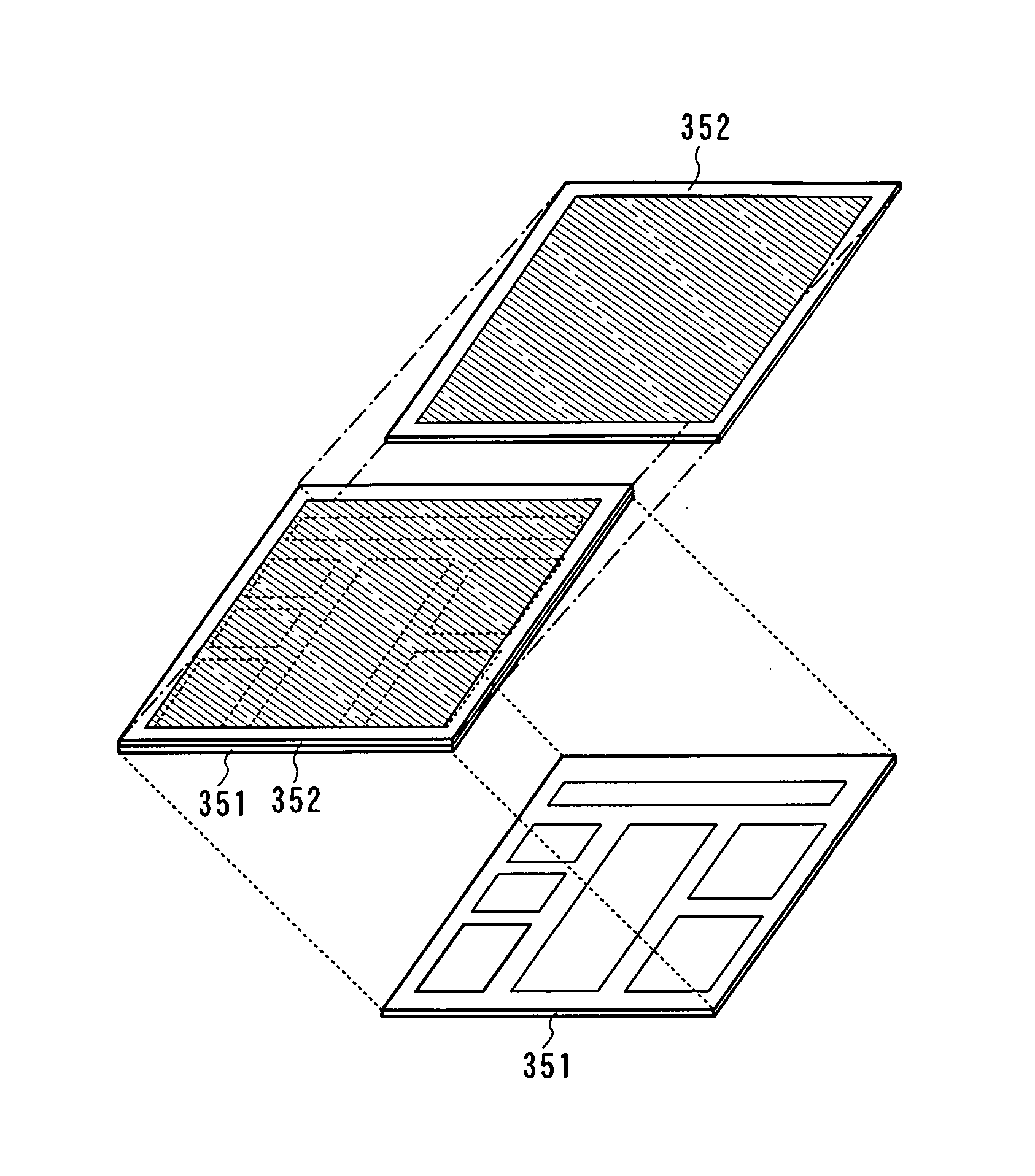
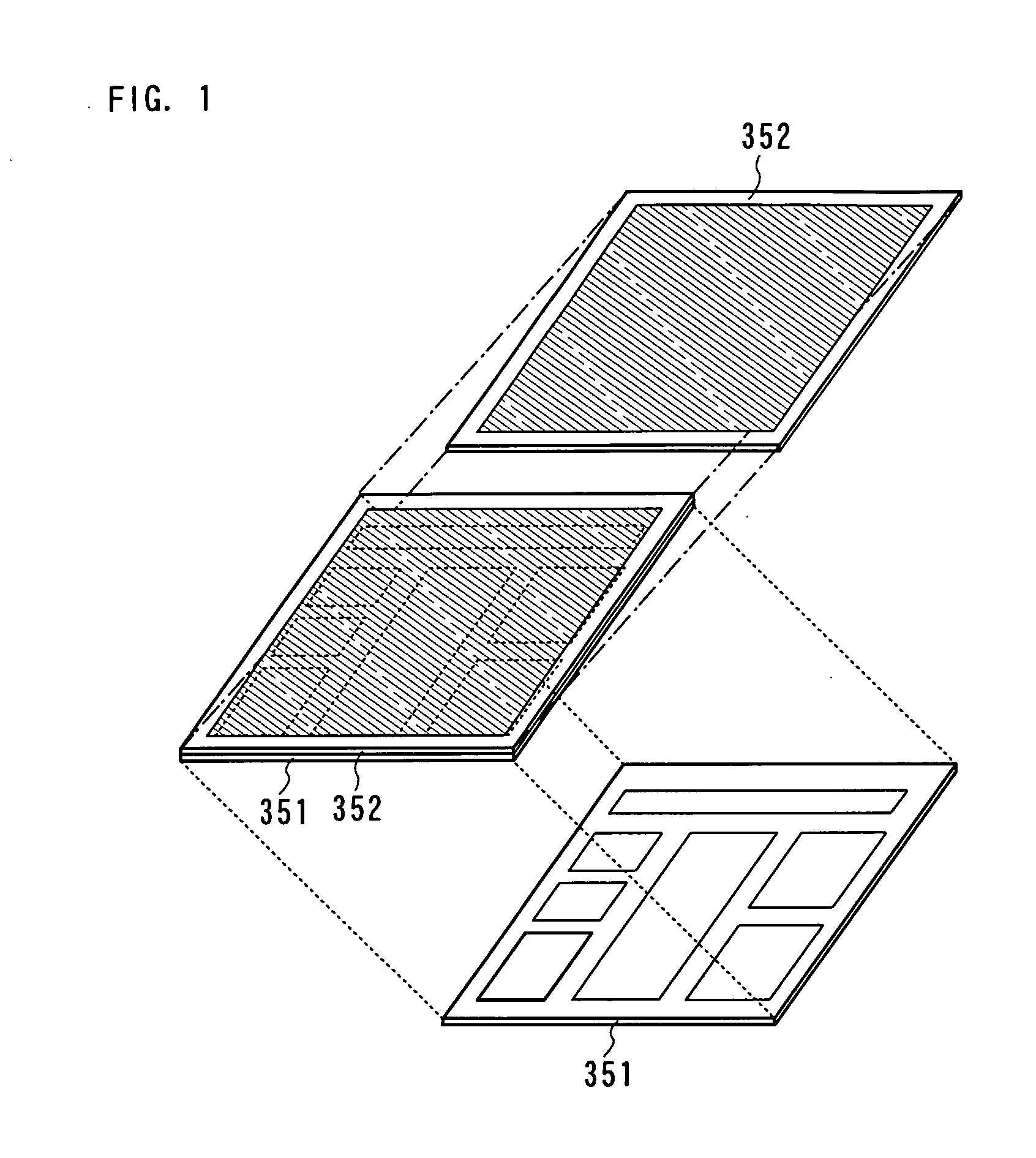
[0046] A semiconductor device according to the invention has a structure in which a plurality of circuits is integrated, which includes a layer 351 including a plurality of field effect transistors (FETs) and a layer 352 including a plurality of memory elements are sequentially stacked (FIG. 1). Various circuits are configured by the layer 351 including a plurality of field effect transistors, and the layer 352 including the plurality of memory elements has a memory circuit for storing data.
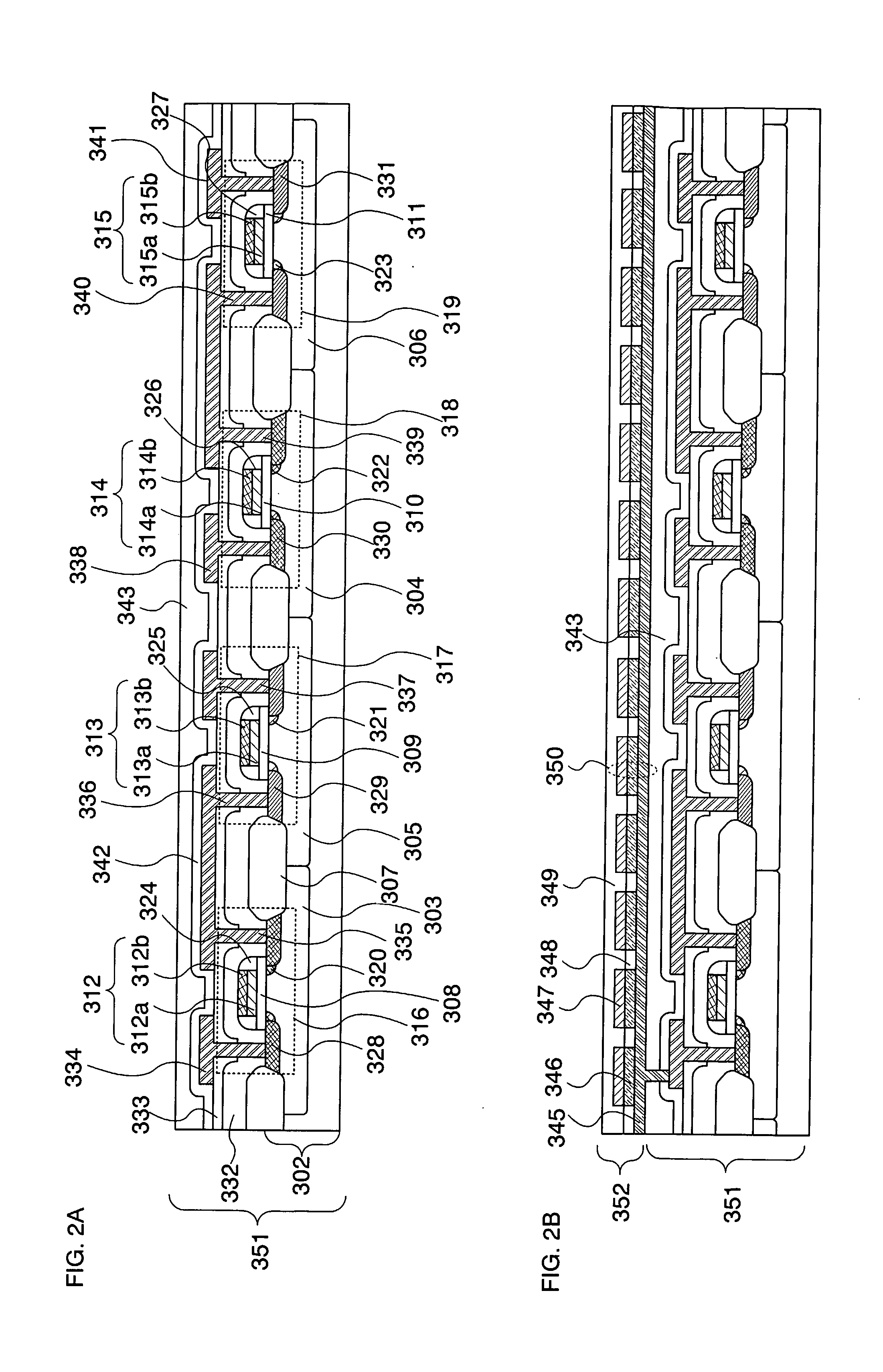
[0047] Next, the cross-sectional structure of a semiconductor device having the above structure is explained. First, the cross-sectional structure of the layer 351 including a plurality of field effect transistors is explained (FIG. 2A).
[0081] In this embodiment mode, the structure of a memory element shown in Embodiment Mode 1 is explained hereinafter.
[0082] The present invention has a feature that the memory element (hereinafter, also referred to as an organic memory element) shown in the above embodiment mode includes an organic compound layer. A memory may include only an organic memory element or may include other memory element. A memory including an organic memory element (hereinafter, also referred to as an organic memory) utilizes the material of an organic compound and makes electric resistance change by optical action or by electric action to the organic compound layer.
[0083] The structure of the organic memory is explained with reference to FIG. 13. The organic memory includes a memory cell array 22 provided with a plurality of memory cells 21 in a matrix, decoders 23 and 24, a selector 25, and a reading / writing circuit 26. The structure of the organic memory shown in FIG. 13 corresponds to the struct...
embodiment mode 3
[0113] As described above, a memory is an indispensable component of a semiconductor device according to the present invention. In this embodiment mode, a memory which has different structure from that of the above Embodiment Mode 2 is explained with reference to FIGS. 11A to 11C.
[0114] A memory 216 includes a memory cell array 222 provided with memory cells 221 in a matrix, decoders 223 and 224, a selector 225, and a reading / writing circuit 226 in FIG. 11A. The structure of the memory 216 here is one example, and other circuits such as a sense amplifier, an output circuit, a buffer, and the like may be included.
[0115] The memory cell 221 includes a first wiring connected to a bit line Bx (1≦x≦m), a second wiring connected to a word line Wy (1≦y≦n), a transistor 240, and a memory element 241. The memory element 241 has a structure in which an organic compound layer is interposed between a pair of conductive layers. A gate electrode of the transistor is connected to the word line, ...
PUM
Abstract
It is an object of the present invention to provide a semiconductor device in which data can be written except when manufacturing the semiconductor device and that counterfeits can be prevented. Moreover, it is another object of the invention to provide an inexpensive semiconductor device including a memory having a simple structure. The semiconductor device includes a field effecttransistor formed over a single crystal semiconductor substrate, a first conductive layer formed over the field effecttransistor, an organic compound layer formed over the first conductive layer, and a second conductive layer formed over the organic compound layer, and a memory element includes the first conductive layer, the organic compound, and the second conductive layer. According to the above structure, a semiconductor device which can conduct non-contact transmission / reception of data can be provided by possessing an antenna.
Description
TECHNICAL FIELD [0001] The present invention relates to a semiconductor device having a memory element. More specifically, the invention relates to a semiconductor device including an organic compound layer as the memory element. BACKGROUND ART [0002] In recent years, electronic devices using organic materials are widely developed, and organic ELs which are light emitting elements, organic TFTs, and the like are developed. In addition, memory elements using organic materials, for example, mask ROMs and the like utilizing organic diodes, are studied (for example, Patent Document 1: Japanese Patent Publication No. 2001-516964). In these memory elements, writing (writing once, reading many) data cannot be conducted except when manufacturing the memory element; therefore, the memory elements are inconvenient. DISCLOSURE OF INVENTION [0003] It is an object of the present invention to provide a semiconductor device in which data can be written except when manufacturing a chip and that cou...
Claims
Application Information
Patent Timeline
Application Date:The date an application was filed.
Publication Date:The date a patent or application was officially published.
First Publication Date:The earliest publication date of a patent with the same application number.
Issue Date:Publication date of the patent grant document.
PCT Entry Date:The Entry date of PCT National Phase.
Estimated Expiry Date:The statutory expiry date of a patent right according to the Patent Law, and it is the longest term of protection that the patent right can achieve without the termination of the patent right due to other reasons(Term extension factor has been taken into account ).
Invalid Date:Actual expiry date is based on effective date or publication date of legal transaction data of invalid patent.

