
Optical functional devices

a functional device and optical technology, applied in the field of optical functional devices, can solve the problems of substantially limited operation speed, achieve the effect of preventing light wave leakage, reducing the effective refractive index nm, and reducing the cost of operation

Active Publication Date: 2008-02-28
NGK INSULATORS LTD
View PDF7 Cites 18 Cited by
  • Summary
  • Abstract
  • Description
  • Claims
  • Application Information

AI Technical Summary

Benefits of technology

[0015]An object of the present invention is to provide an optical modulator having superior properties as photonic crystal and capable of high-speed operation by improving the structure of the modulator.
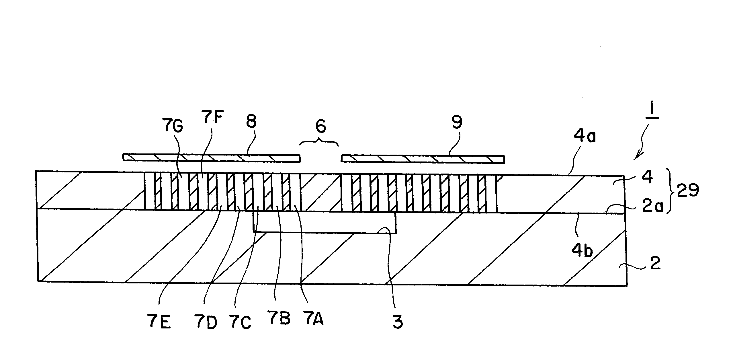
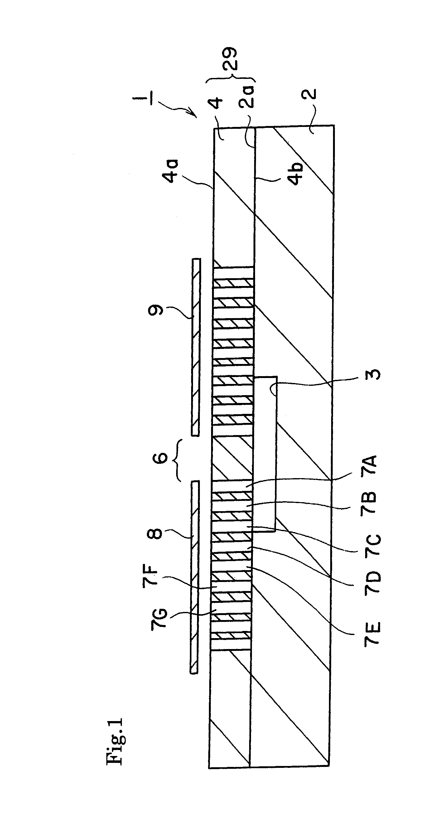
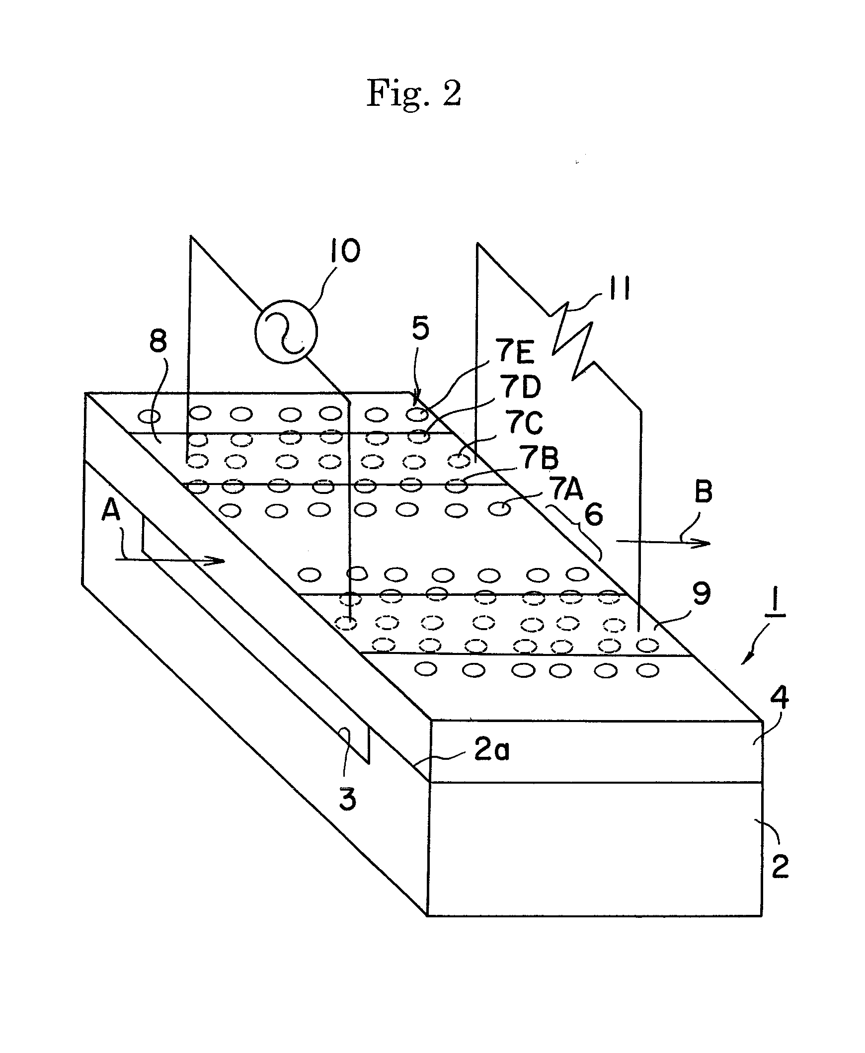
[0021]According to the present invention, the layer of a high dielectric constant is laminated onto the dielectric layer. It is thereby possible to considerably raises the effective refractive index Nm of signal wave propagating in the traveling type electrode and thus attain velocity matching of the refractive index of signal electrode and the optical group refractive index GNo. The modulation band can be thus widened. At the same time, the low dielectric portion is provided, to which lattice columns of at least first to third orders in distance with respect to the waveguide portion faces. It is thus possible to prevent leakage of light wave into the layer of high refractive index and to reduce the propagation loss of the light wave at a practical level. As described above, the present invention enables wide band modulation in a field of an optical modulator using a slab-type photonic crystal. The practical benefits in the industry are thus quite considerable.

Problems solved by technology

It is thus proved that the operating velocity is substantially limited due to the velocity mismatch of microwave and light wave.

Method used


Image

  • Optical functional devices
  • Optical functional devices
  • Optical functional devices

Examples


example 1

[0094]The optical modulating devices of the examples of FIGS. 8, 9 and 10 were tested. It was further tested for an optical modulator that the layer of high dielectric constant was not provided under the lattice columns in FIG. 8. The effective refractive index Nm of microwave applied on the modulating electrodes was calculated by simulation for each device. It was provided that the dielectric layer 4 was made of lithium niobate single crystal and the refractive index Nhs of the layer 2 (substrate) of high refractive index was changed as shown in FIG. 14. The results were shown in FIG. 14. Further, the parameters were as follows.[0095]Optical modulator of FIG. 8: type A[0096]Optical modulator of FIG. 9: type B[0097]Optical modulator of FIG. 10: type C[0098]Optical modulator that the layer of high dielectric constant is not provided[0099]under the lattice column: prior type[0100]Thickness tsub of dielectric film slab: 0.4 μm[0101]Thickness tm of ground and signal electrodes: 1 μm[010...

example 2

[0106]The dependency of the effective refractive index Nm of microwave on (WgI·G) / 2(=ΔWgI) was tested for the optical modulator of FIG. 10. WgI represents the width of the low dielectric portion, and G represents the electrode gap and 5 μm. The width W of the central and signal electrode was made 10 μm, 20 μm or infinite value. A WgI is an indicator showing the distance of the layer of high dielectric constant and the electrode edge viewed horizontally.

[0107]The effective refractive index Nm of microwave applied on the modulating electrodes was calculated by simulation for this device. It was provided that the dielectric layer 4 was made of lithium niobate single crystal. The parameters were as follows. The results were shown in FIG. 15.[0108]Thickness tsub of dielectric layer: 0.4 μm[0109]Thickness of ground and signal electrodes: 1 μm[0110]Electrode gap G: 5 μm[0111]Width W of signal electrode: 10 μm, 20 μm or infinite value[0112]Width WgI of low dielectric portion: 5 μm[0113]Dept...

example 3

[0115]The dependency of the refractive index Nm of microwave on the thickness tm of of the ground and signal electrodes was tested for the optical modulator of FIG. 10. The effective refractive index Nm of microwave applied on the modulating electrodes was calculated by simulation for this device. It was provided that the dielectric layer 4 was made of lithium niobate single crystal. The parameters were as follows. The results were shown in FIG. 16.[0116]Thickness tsub of dielectric layer: 0.4 μm[0117]Thickness tm of ground and signal electrodes: 1, 3 or 10 μm[0118]Electrode gap: 5 μm[0119]Width W of signal electrode: 10 μm[0120]Width WgI of low dielectric portion: 5 μm[0121]Depth ths of low dielectric portion: 1 μm

[0122]As a result, it was proved that the effective refractive index of microwave can be further improved by lowering the thickness tm of the ground and signal electrodes. On this viewpoint, the thickness tm of the ground or signal electrode may preferably be 10 μm or sma...


PUM


Abstract

An optical functional device 1 has a slab type two-dimensional photonic crystal layer 29. The layer 29 has a dielectric layer 4 and a plurality of lattice columns 5 each comprising dielectric pillars. A waveguide portion 6 is provided in the photonic crystal layer 29. A ground electrode 8 and a signal electrode 9 are formed on the dielectric layer 4 for applying a modulating voltage on light propagating in the waveguide portion 6. A layer 2 of a high dielectric constant is laminated on the dielectric layer 4. A low dielectric portion is formed direct under the waveguide portion 6 and the lattice columns 7a, 7B and 7C of at least first, second and third orders in distance with respect to said waveguide portion.

Description

[0001]This application claims the benefit of Japanese Patent Application P2006-229213 filed on Aug. 25, 2006, the entirety of which is incorporated by reference.BACKGROUND OF THE INVENTION[0002]1. Field of the Invention[0003]The present invention relates to an optical functional device utilizing a slab-type and two-dimensional photonic crystal.[0004]2. Related Art Statement[0005]An optical device utilizing a photonic crystal has a structure of repeating different two kinds of dielectric materials having different dielectric constants. According to such devices, the internal multiple reflection phenomenon is utilized to provide various kinds of devices having superior functions and of very small sizes. Since the principle of function of the device is based on multiple reflection phenomenon, the device properties have a strong dependency on frequency (wavelength) in the vicinity of a specific frequency. The frequency is decided upon the material (refractive index N) of a substrate for...

Claims


Application Information

Patent Timeline
Patent Type & Authority Applications(United States)
IPC IPC(8): G02B6/10
CPCG02F1/0356G02F2202/32G02F2001/212G02F1/2255G02F1/212
Inventor MITOMI, OSAMUIWATA, YUICHIKONDO, JUNGOAOKI, KENJIEJIRI, TETSUYA
Owner NGK INSULATORS LTD
Learn More