Manufacturing of flexible display device panel

a flexible display and panel technology, applied in the field of display panels, can solve the problems of inconvenient portability and large-scale display, low performance of tft formed by low temperature deposition, and easy warpage of plastic substrates

Inactive Publication Date: 2008-02-28
SAMSUNG ELECTRONICS CO LTD
View PDF10 Cites 205 Cited by
  • Summary
  • Abstract
  • Description
  • Claims
  • Application Information

AI Technical Summary

Problems solved by technology

However, because such a display device uses a heavy and fragile glass substrate, it is not suitable for portable and large scale displays.
However, the plastic substrate is easily warped by the high temperature used during the manufacturing process and therefore thin film transistors that may be deposited at a low temperature are used to prevent deformation of the plastic substrate.
However, the performance of the TFT formed by low temperature deposition may not as high as desired.

Method used


Image

  • Manufacturing of flexible display device panel
  • Manufacturing of flexible display device panel
  • Manufacturing of flexible display device panel

Examples


Embodiment Construction

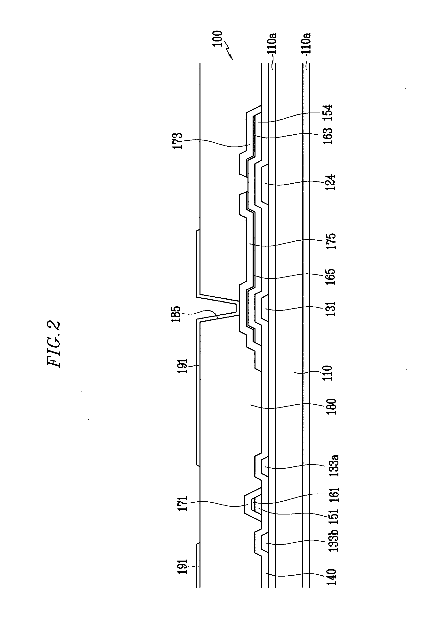
[0032]In the drawings, the thickness of layers, films, panels, regions, etc., are exaggerated for clarity. It will be understood that when an element such as a layer, film, region, or substrate is referred to as being “on” another element, it can be directly on the other element or intervening elements may also be present. In contrast, when an element is referred to as being “directly on” another element, there are no intervening elements present.

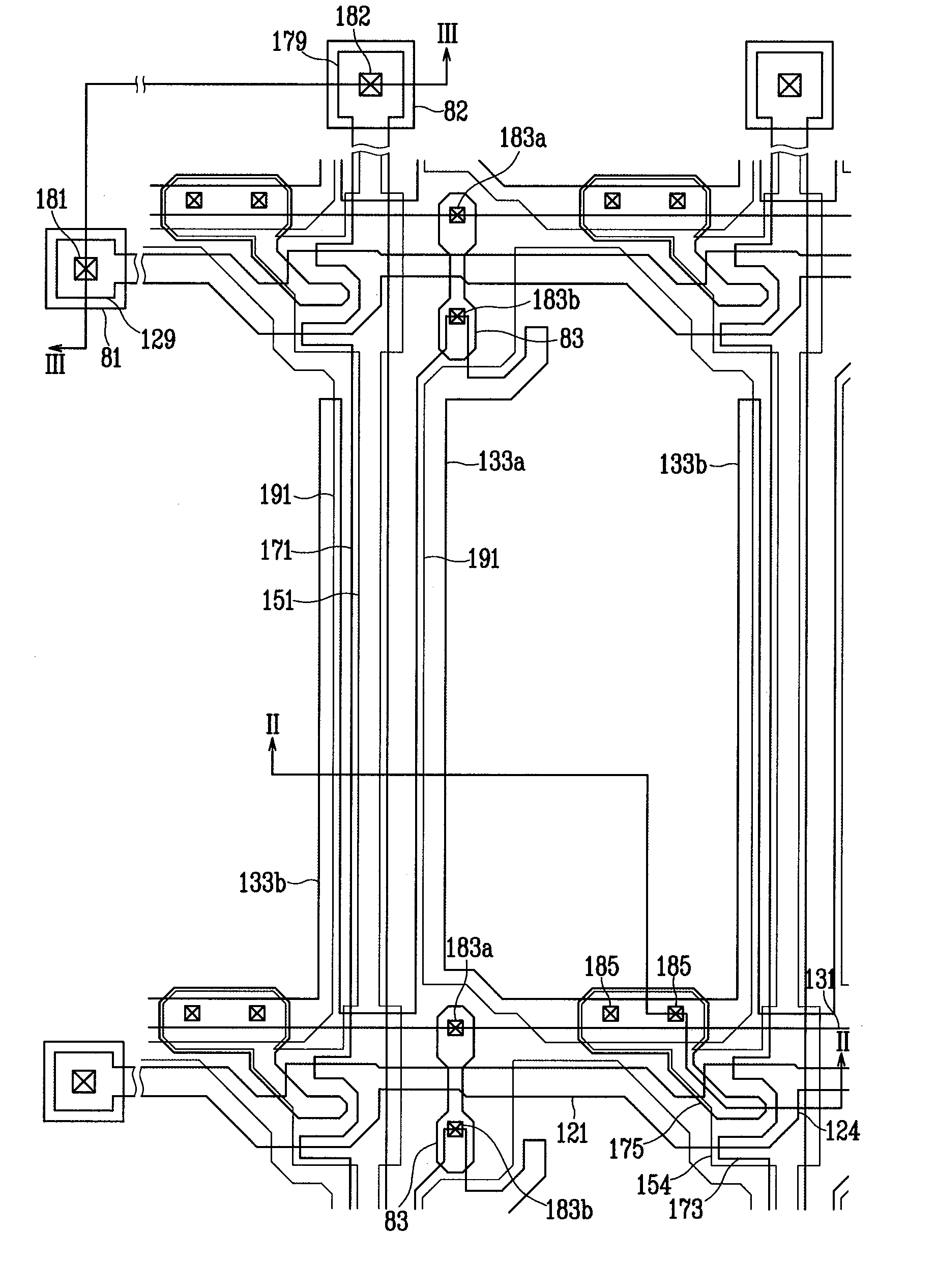
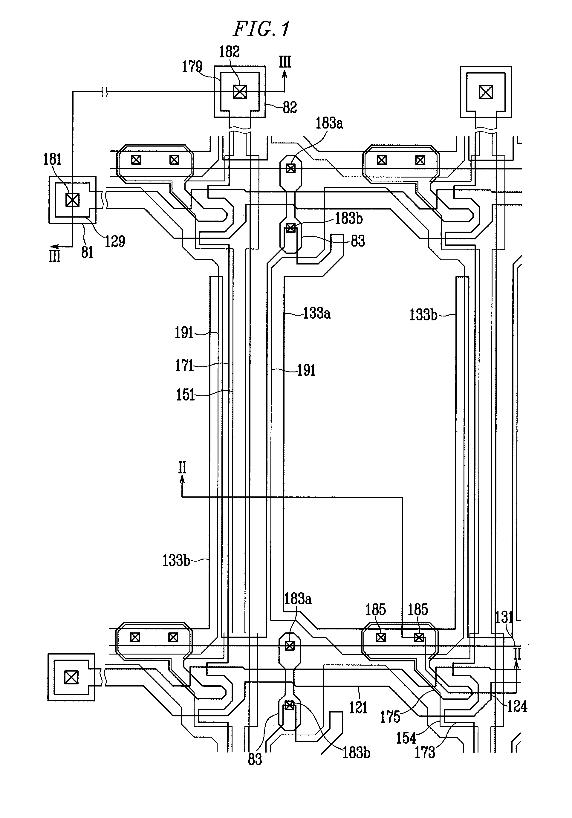
[0033]First, a thin film transistor (TFT) array panel according to an embodiment of the present invention will be described in detail with reference to FIG. 1 to FIG. 3.

[0034]FIG. 1 is a layout view of a TFT array panel according to an embodiment of the present invention, and FIG. 2 and FIG. 3 are sectional views of the TFT array panel shown in FIG. 1 taken along the lines II-II and III-III, respectively.

[0035]A plurality of gate lines 121 and a plurality of storage electrode lines 131 are formed on a flexible insulating substrate 110.

[0036...


PUM

PropertyMeasurementUnit
RF poweraaaaaaaaaa
RF poweraaaaaaaaaa
temperatureaaaaaaaaaa

Abstract

A manufacturing method of a display panel for an LCD includes forming a gate line on a flexible insulation substrate, depositing a gate insulating layer on the gate line, forming a semiconductor layer on the gate insulating layer and forming a data line and a drain electrode on the semiconductor layer and the gate insulating layer. The forming the semiconductor layer may be performed by PECVD at about 100° C. to about 180° C., the gate insulating layer may have a thickness of about 2000 Å to about 5500. The method may further include performing hydrogen plasma treatment on the gate insulating layer after the depositing the gate insulating layer and annealing the substrate having the plurality of thin films after the forming the data line and the drain electrode. The insulation substrate may include PES.

Description

CROSS-REFERENCE TO RELATED APPLICATION[0001]This application claims priority to and the benefit of Korean Patent Application No. 10-2006-0079911 filed in the Korean Intellectual Property Office on Aug. 23, 2006, the entire contents of which are incorporated herein by reference.BACKGROUND OF THE INVENTION[0002]1. Field of the Invention[0003]The present invention relates to a display panel for a flexible display device and a manufacturing method thereof.[0004]2. Description of the Related Art[0005]Liquid crystal and organic light emitting diode (OLED) displays are representative of flat panel displays that are used widely. The liquid crystal display generally includes an upper panel in which a common electrode, color filters, etc., are formed, a lower panel in which thin film transistors (TFTs) and pixel electrodes are formed. A liquid crystal layer is interposed between the two display panels. If a potential difference is applied between a pixel electrode and the common electrode, th...

Claims


Application Information

Patent Timeline
Patent Type & Authority Applications(United States)
IPC IPC(8): H01L21/441H01L33/00G02F1/1368G09F9/00G09F9/30H01L21/205H01L21/336H01L29/786
CPCG02F1/1368H01L29/78603H01L27/1214H01L27/127H01L27/1218H01L21/2053H01L29/4908
Inventor HWANG, TAE-HYUNGNIKULIN, IVANJEON, HYUNG-ILKIM, SANG-IIROH, NAM-SEOK
Owner SAMSUNG ELECTRONICS CO LTD
Why Eureka
Try Eureka