Dry etching method

a technology of dry etching and etching plate, which is applied in the direction of basic electric elements, semiconductor/solid-state device manufacturing, electric devices, etc., can solve the problems of undetected etching shape, increased resistance thickness, and increased resistance selectivity, so as to achieve high resist selectivity and high speed

Inactive Publication Date: 2008-02-28
PANASONIC CORP
View PDF10 Cites 10 Cited by
  • Summary
  • Abstract
  • Description
  • Claims
  • Application Information

AI Technical Summary

Benefits of technology

[0028]In view of the foregoing, the present invention has its object of increasing resist selectivity in etching an insulating film of which main compositions are Si and C.
[0049]In short, the present invention relating to a dry etching method using plasma achieves increased resist selectivity especially when applied to etching of an insulating film of which main compositions are Si and C and is very useful therefore.

Problems solved by technology

When an insulting film of which main compositions are Si and C, such as a SiOC film or the like is etched, especially, when such an insulating film is etched with the use of a resist for ArF exposure, however, undesirable reduction in thickness of the resist by etching is caused due to low resist selectivity, as described above, resulting in an undesirably etched shape (see FIG. 9D).
This problem is more significant in over-etching that is practically performed in the present day.
Moreover, the above described problems become more significant when the initial film thicknesses of resists become smaller in association with progress in miniaturization.

Method used


Image

  • Dry etching method
  • Dry etching method
  • Dry etching method

Examples


embodiment 1

[0060]A dry etching method according to Embodiment 1 of the present invention will be described with reference to the drawings by referring to the case where a to-be-etched film is a SiOC film.

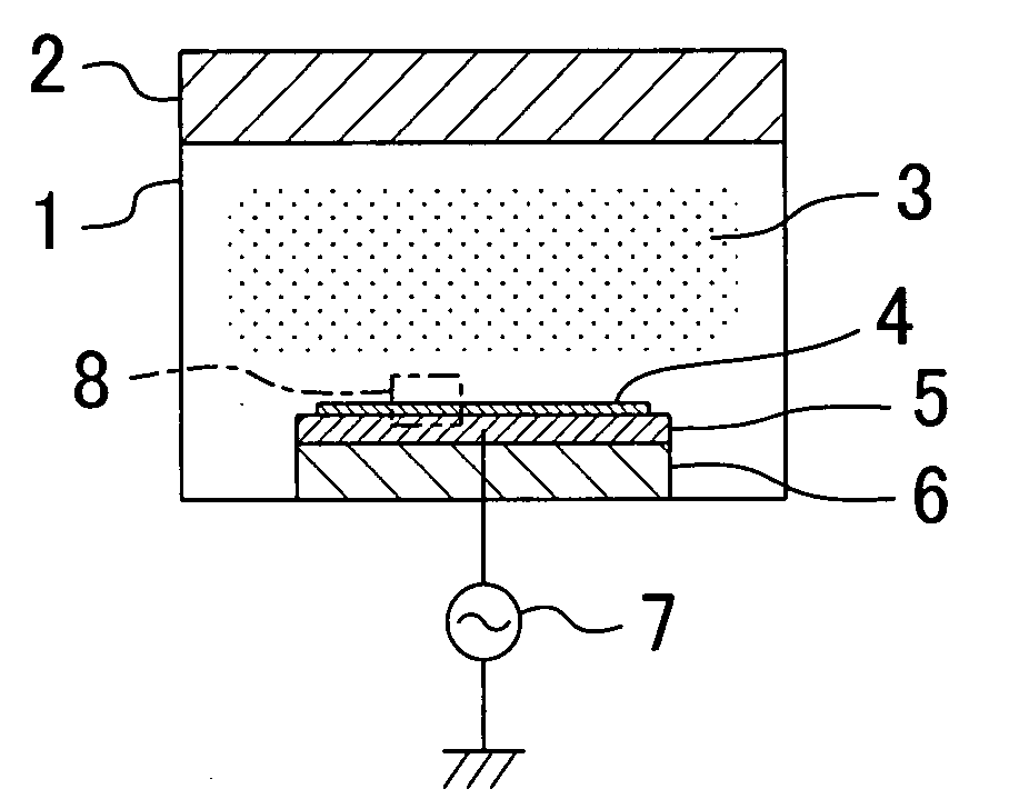
[0061]FIG. 1A is a schematic configuration diagram of a dry etching apparatus for performing the dry etching method according to the present embodiment.

[0062]In the dry etching apparatus used in the present embodiment shown in FIG. 1A, a plasma source 2 for generating plasma 3 is provided at the upper part of a vacuum reaction chamber 1 capable of keeping a reduced pressure state by generating constant gas flow while an electrode 5 for holding a wafer 4 is provided at the lower part of the vacuum reaction chamber 1. An insulator 6 intervenes between the electrode 5 and the bottom of the vacuum reaction chamber 1, and the electrode 5 is connected to an RF power source 7 used as an RF bias generating source for extracting ions from the plasma 3.

[0063]The plasma source 2 may be a capacitive coupl...

embodiment 2

[0141]A dry etching method according to Embodiment 2 of the present invention will be described with reference to the drawings by referring to the case using a SiOC film as a to-be-etched film.

[0142]In the present embodiment, similarly to Embodiment 1, for dry etching an insulating film of which main compositions are Si and C, such as a SiOC film or the like, a low frequency RF bias of 2 MHz or lower is applied to an electrode on which a wafer is placed while plasma is generated from a mixed gas of a molecule gas containing carbon and fluorine and a molecule gas containing nitrogen.

[0143]Difference of the present embodiment from Embodiment 1 lies in that the RF bias power is set to, for example, 250 W to set the maximum energy of incident ions to the insulating film from the plasma by the RF bias to 600 eV or lower. Specifically, etching conditions of the present embodiment (etching conditions 3 of the present invention) are the same as those of the etching conditions in Embodiment ...


PUM


Abstract

In dry etching an insulating film containing silicon and carbon and formed on a wafer, plasma is generated from a mixed gas of a first molecule gas containing carbon and fluorine and a second molecule gas containing nitrogen. At this time, an RF bias of 2 MHz or lower is applied to an electrode on which the wafer is placed.

Description

FIELD OF THE INVENTION [0001]The present invention relates to dry etching methods, and particularly relates to a method for etching an insulating film of which main compositions are Si and C.BACKGROUND ART [0002]In recent years, low dielectric constant insulating films (low-k films) are used as insulating films for wirings for improving circuit delay accompanied by miniaturization of semiconductor integrated circuit devices. Presently, in CMOS (Complementary Metal-Oxide Semiconductor) devices under 65 nm design rule, SiOC films are used widely as the low-k films. For etching SiOC films, resists for ArF exposure are used.[0003]The resists for ArF exposure, however, involve a disadvantage of low etching resistance.[0004]A conventional SiOC film dry etching method will be described with reference to FIG. 9A to FIG. 9D.[0005]In general, a dry etching apparatus shown in FIG. 9A includes a vacuum reaction chamber 101 capable of keeping a reduced pressure state by generating constant gas f...

Claims


Application Information

Patent Timeline
Patent Type & Authority Applications(United States)
IPC IPC(8): H01L21/302
CPCH01L21/31116
Inventor NAKAGAWA, HIDEO
Owner PANASONIC CORP
Why Eureka
Try Eureka