Method to eliminate striations and surface roughness caused by dry etch

a technology of dry etching and surface roughness, which is applied in the direction of decorative surface effects, electrical equipment, decorative arts, etc., can solve the problems of etch features that are prone to striation, surface roughness and striation, and the resist layer gradually erodes away, so as to inhibit the erosion of the mask layer, and reduce the resist etching rate

Inactive Publication Date: 2006-12-26
MICRON TECH INC
View PDF21 Cites 38 Cited by
  • Summary
  • Abstract
  • Description
  • Claims
  • Application Information

AI Technical Summary

Benefits of technology

[0014]A second etching is then performed by exposing the silicon oxide layer to a second etch gas to increase the opening downwardly through the silicon oxide layer while a polymeric material is formed on the mask layer during the etching step. The second etch gas includes at least one organic fluorocarbon and an effective amount of at least one nitrogen-comprising gas to reduce the resist etch rate and / or provide formation of polymeric material on the mask layer during the etching step. The second etch gas can be provided as a separate gas or by increasing the amount of the nitrogen-comprising gas of the first etch gas to reduce the etch rate of the resist and / or deposit polymeric material on the mask during the etching step to inhibit erosion of the mask layer. Upon depositing a layer of the polymeric material that protects the photomask layer opening, the silicon oxide layer can be further etched to increase the depth of the opening by exposing the oxide layer to the first etch gas, or by decreasing the amount of the nitrogen-comprising gas in the second etch gas to a level whereby formation of polymeric material on the mask is substantially suppressed during the etching step.
[0015]In another embodiment of the invention, the method involves etching a contact opening through a silicon oxide layer by exposing the silicon oxide layer to a first etch gas to partially etch the opening while a polymeric material is formed on the surface of the mask, and then to a second etch gas to further extend the opening downward while suppressing deposition of the polymeric material. The first etch gas includes at least one organic fluorocarbon and an effective amount of at least one nitrogen-comprising gas to reduce the etch rate of the resist and / or provide formation of polymeric material on the mask layer during the etching step to help maintain the thickness of the mask layer on the silicon oxide layer.
[0016]Upon depositing a layer of the polymeric material that protects the photoresist mask or inhibits etching of the photoresist mask, a second etching is performed to extend the opening downwardly by decreasing the amount of the nitrogen-comprising gas in the etch gas or applying a second etch gas that includes at least one organic fluorocarbon and, optionally, a minor amount of one or more nitrogen-comprising gases, whereby formation of polymeric material on the mask is substantially suppressed during the etching step. Upon reducing the layer of polymeric material whereby the contact opening is unconstricted, the silicon oxide layer can be further etched to increase the depth of the opening by exposing the oxide layer to the first etch gas, or by increasing the amount of the nitrogen-comprising gas to reduce the etch rate of the resist and / or deposit polymeric material on the mask during the etching step to inhibit erosion of the mask layer.
[0017]It was found that the addition of a nitrogen-comprising gas such as NH3 to the fluorocarbon etch gas helps maintain the smoothness of the surface of the resist layer to eliminate striations in the etch features, helps eliminate faceting and erosion of the mask and increases the resist selectivity, i.e., decreases the photoresist etch rate with respect to the oxide etch rate. Advantageously, the present invention provides a method for achieving an anistropic etch of an oxide layer to provide a contact opening having a high aspect ratio of at least about 5:1 by using and controlling the amount of polymeric material that forms on the mask layer from the etch gases to maintain the integrity of the mask throughout the etch process to help control the resolution or dimension of the diameter of the contact opening.

Problems solved by technology

Although the plasma etch rate of the oxide is generally faster than the resist erosion rate, when dry etching an opening having a high aspect ratio, the etch chemistry causes the resist layer to gradually erode away, often before the desired depth of the opening is achieved.
Another problem is related to faceting or chaffering of the photoresist mask at the edge of the opening, caused by ion bombardment.
This can wear away the underlying oxide resulting in surface roughness and striations in the etch features, and the loss of critical dimensions of the opening being etched.
In an array such as a memory cell, contacts are positioned in close proximity to each other, and the erosion and localized breakdown of the photoresist can result in the development of notches and other blemishes in the surface of the contact, which can extend to and short an adjacent contact.

Method used


Image

  • Method to eliminate striations and surface roughness caused by dry etch
  • Method to eliminate striations and surface roughness caused by dry etch
  • Method to eliminate striations and surface roughness caused by dry etch

Examples


example

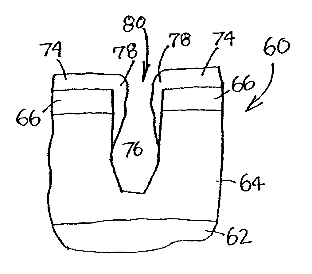
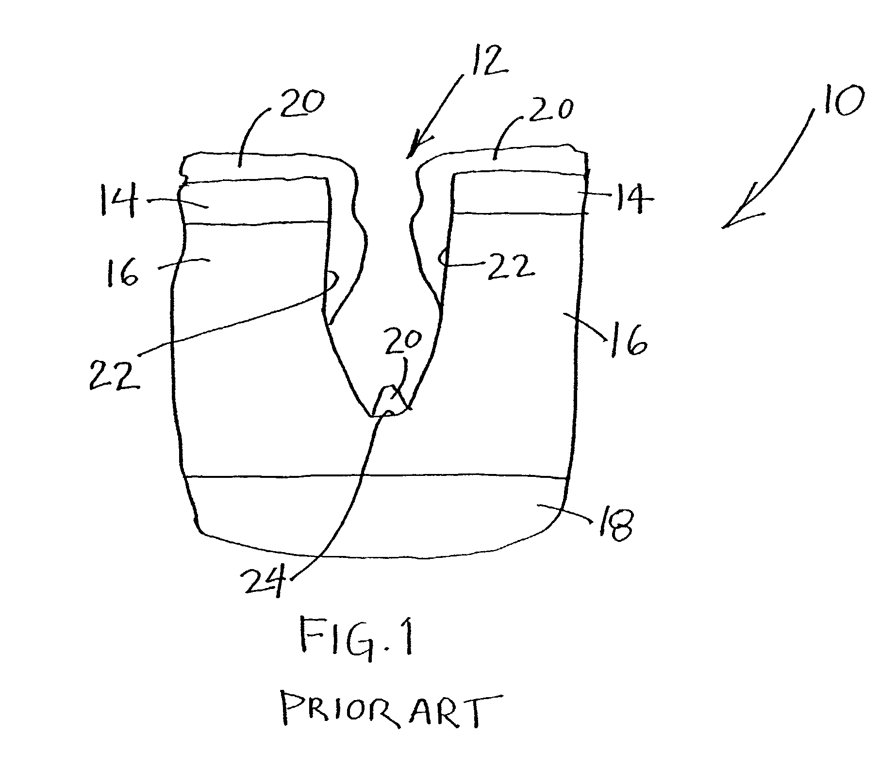
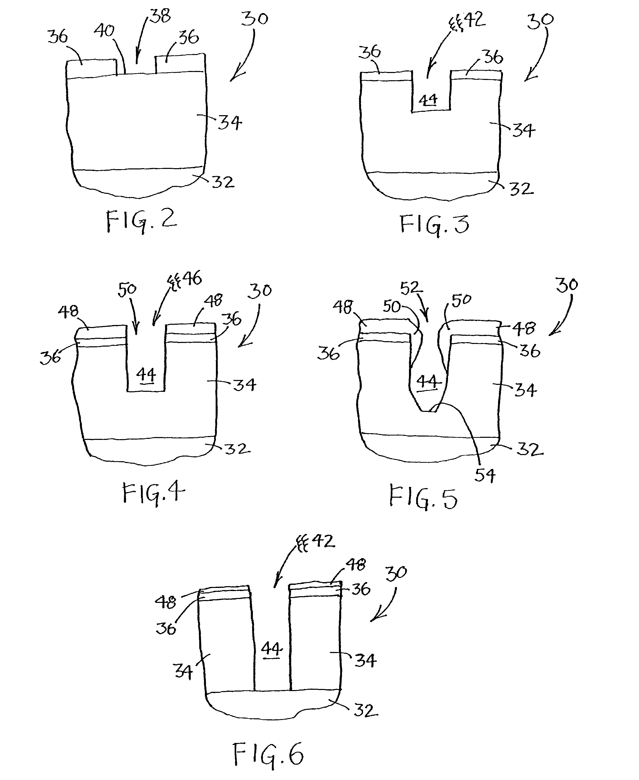
[0050]A wafer having a 20,000 angstroms layer of BPSG masked with a 7,600 angstroms layer of JSR-KRF-MISG (DUV) photoresist were etched in a MERIE etch chamber using a hydrofluorocarbon and fluorocarbon plasma with and without the addition of ammonia (NH3) to form contact openings through the oxide layer.

[0051]A first wafer (control wafer) was etched using a feed gas of 50 sccm CHF3, 25 sccm CF4, and 100 sccm Ar, at a pressure of 50 mTorr, power of 900 watts, ESC temperature of 10 C., and a time duration of 180 seconds. FIG. 12a shows a cross-sectional view of the resultant oxide layer with openings etched to a depth of about 7,100 angstroms. The thickness of the resist layer remaining after the etch was about 6,000 angstroms. FIG. 12b is a cross-sectional and oblique view of the surface of the etched oxide with overlying resist layer, showing the surface roughness of the resist. Such roughness has resulted in the development of striations at the top portion of a high aspect ratio e...


PUM

PropertyMeasurementUnit
depthaaaaaaaaaa
pressureaaaaaaaaaa
power levelaaaaaaaaaa

Abstract

A plasma etch process for forming a high aspect ratio contact opening through a silicon oxide layer is disclosed. The silicon oxide layer is plasma etched using etch gases that include at least one organic fluorocarbon gas. At least one etch gas is used that includes one or more nitrogen-comprising gases to deposit a surface polymeric material during the etching for maintaining a masking layer over the silicon oxide layer. The method of the invention achieves a complete and anistropic etching of a contact opening having a high aspect ratio and the desired dimensions.

Description

[0001]This application is a Continuation of patent application Ser. No. 09 / 652,835 filed on Aug. 31, 2000 now U.S. Pat. 6,569,774.FIELD OF THE INVENTION[0002]The present invention relates to the field of semiconductor device fabrication, and more particularly to improved methods for etching high aspect ratio contact openings in oxide layers.BACKGROUND OF THE INVENTION[0003]In the fabrication of semiconductor devices, numerous conductive device regions and layers are formed in or on a semiconductor substrate. The conductive regions and layers of the device are isolated from one another by a dielectric or insulating layer, for example, silicon dioxide or a doped oxide such as phosphosilicate glass (PSG) and borophosphosilicate glass (BPSG). These dielectric layers typically overlay a silicon-comprising surface such as single crystal silicon, epitaxial silicon, polysilicon, or silicides such as titanium silicide.[0004]At several stages during wafer fabrication, it is necessary to form ...

Claims


Application Information

Patent Timeline
Patent Type & Authority Patents(United States)
IPC IPC(8): H01L21/302H01L21/311H01L21/461
CPCH01L21/31116H01L21/31144
Inventor TRAPP, SHANE J
Owner MICRON TECH INC
Why Eureka
Try Eureka