Method of manufacturing semiconductor devices

a manufacturing method and semiconductor technology, applied in the direction of semiconductor devices, basic electric elements, electrical equipment, etc., to achieve the effects of reducing the variation in trimming, high-precision processing, and reducing the amount of overetching

Inactive Publication Date: 2003-03-13
HITACHI LTD
View PDF0 Cites 43 Cited by
  • Summary
  • Abstract
  • Description
  • Claims
  • Application Information

AI Technical Summary

Benefits of technology

0027] According to the present invention, it is possible to reduce variation in trimming and to realize high-precision processing. These objects are achieved by reducing the difference in the amounts of overetching at the step arising from the STI process by minimizing the amount of overetching for BARC trimming. Variation in dimensions at the time of BARC etching due to the step arising from STI occurs because the amount of trimming increases on account of insufficient reaction products produced during overetching for BARC trimming. In other words, difference in the amount of overetching causes variation in the amount of trimming.
0028] According to the present invention, it is possible to solve problems arising from ever-increasing complexity in the process for fabrication of semiconductor devices, because the process of the present invention does not need any special mask structure or any change in gate structure.
0029] According to the present invention, it is possible to solve the problems with contamination by foreign matter that occur while wafers are being transferred from one apparatus to another. (Contamination is the major cause to decrease yields.) The solution is achieved by performing mask trimming and gate electrode trimming in a vacuum environment.
0030] According to the present invention, it is possible to solve the problems with decrease in throughput, disposal of washing solution, and increase in cost of ownership (COO), all of which result from the additional cleaning step. This object is achieved because the process of the present invention permits dry cleaning to be performed in a vacuum environment. Dry cleaning in this manner prevents the water absorption of hydrogen halide compounds remaining after dry etching. This permits the wet cleaning to be eliminated or simplified.
0031] According to the present invention, it is possible to control dimensions highly accurately and to realize very small gates (on the order of 50 nm) in high yields. This object is achieved by carrying out the step of inspecting dimensions or contamination in a vacuum environment and feeding the results of inspection to the subsequent steps for their adjustment.
0032] According to the present invention, it is possible to solve the problem with the roughening of resist film patterned by ArF laser. This object is achieved by not exposing wafers to the atmosphere, because the problem arises from hydrolysis in the atmosphere as shown at (603) and (604) in FIG. 6(b).

Problems solved by technology

Variation in dimensions at the time of BARC etching due to the step arising from STI occurs because the amount of trimming increases on account of insufficient reaction products produced during overetching for BARC trimming.

Method used


Image

  • Method of manufacturing semiconductor devices
  • Method of manufacturing semiconductor devices
  • Method of manufacturing semiconductor devices

Examples


example 2

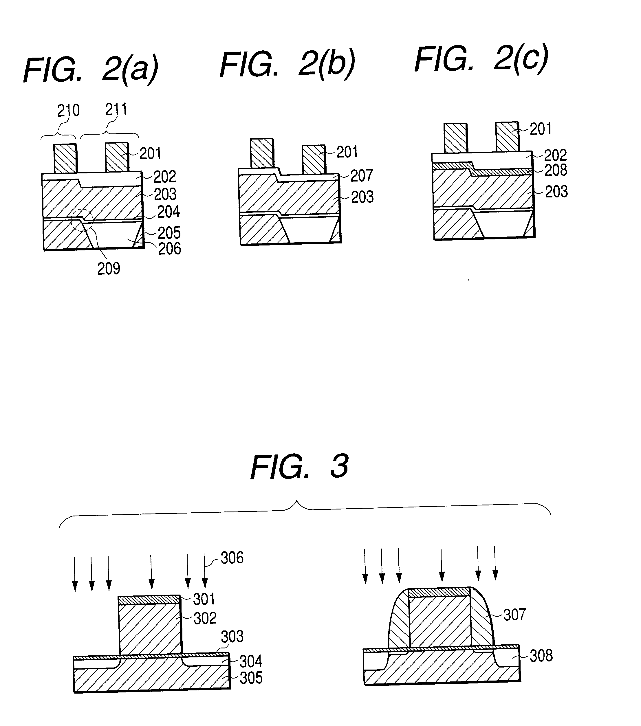
[0062] This example demonstrates a fabrication process in which resist trimming and gate trimming are performed indifferent chambers as shown in FIG. 1(b). The process is intended to realize a gate length of 50 nm from a multi-layered film as shown in FIG. 2(c). This multi-layered film consists of four layers as follows.

[0063] Resist layer (201) . . . 300 nm thick

[0064] BARC layer (202) . . . 65 nm thick

[0065] TEOS layer (208) . . . 50 nm thick

[0066] Poly-Si layer (203) . . . 100 nm thick

[0067] The resist layer has a pattern width of 100 nm formed by exposure to ArF laser. The resist layer (201) needs to remain until the TEOS layer (208) is etched. For the TEOS layer (208) to be etched satisfactorily, the resist layer (201) should have a thickness of 220 nm which is calculated as follows.

50.times.2.times.1.times.2 / 1+20=220 nm Formula (3)

[0068] (where it is assumed that the resist selectivity is 1, the ratio of mask edge to mask center is 2 / 1 (facet factor), TEOS overetching is 100% ...

example 3

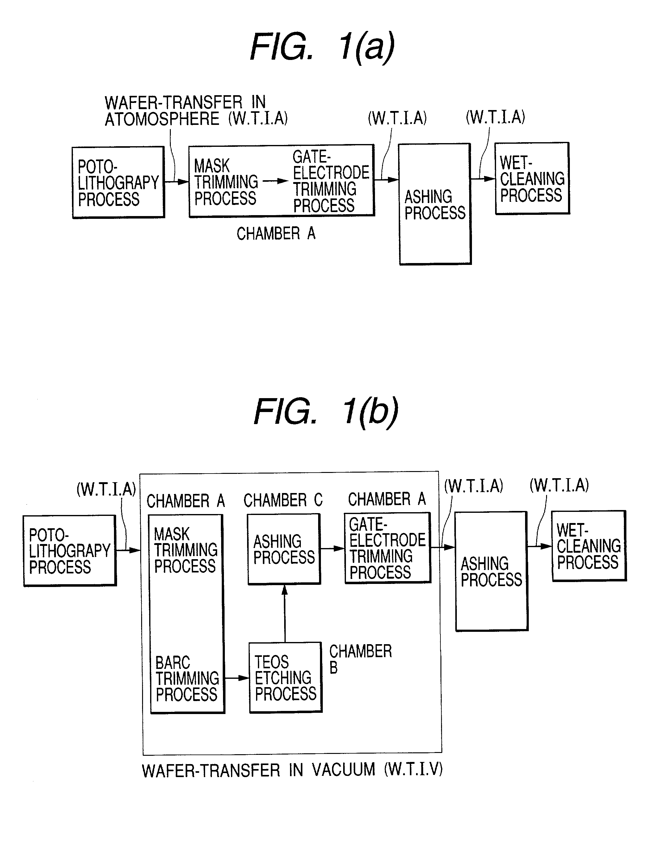
[0087] This example demonstrates the effect of transferring wafers in a vacuum environment throughout all the steps of mask trimming, gate-electrode etching / trimming, ashing, and dry cleaning. Passing wafers through the ashing step without exposure to the atmosphere permits water-absorbing foreign matter to be removed in the case where the gate trimming is carried out by using a hygroscopic halide such as HCl and HBr.

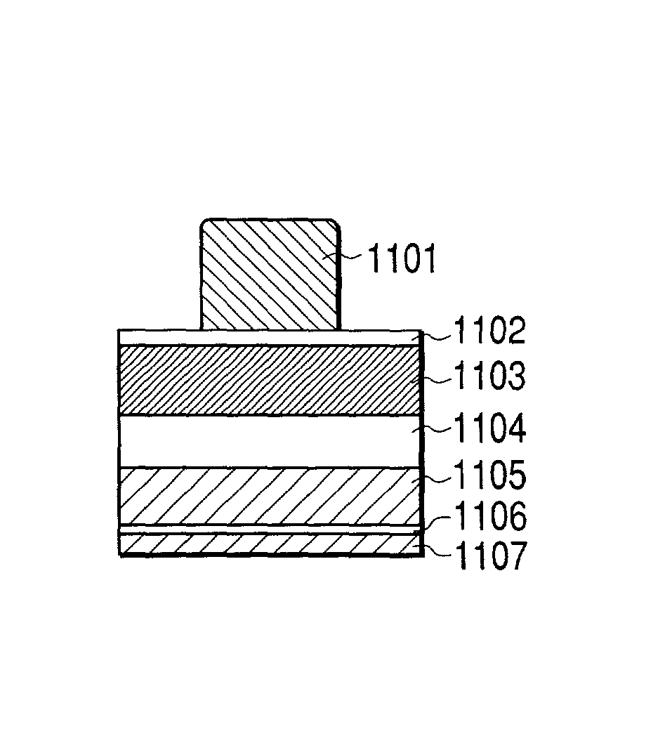
[0088] In this example, the trimming process mentioned in Example 2 was applied to the multi-layered gate consisting of resist (1101), BARC (1102), SiN (1103), W (1104), WN (1105), and poly-Si (1106) on a gate insulating film (1107), as shown in FIG. 11(a). The W layer was etched with plasma containing Cl, O, and N, and the poly-Si layer was etched and trimmed with plasma containing Cl, O, and HBr. The trimmed gate has a shape shown in FIG. 11(b), including SiN (1109), W (1111), and WN (1105). After the etching / trimming step, wafers are transferred in a vacuum environme...

example 4

[0089] The process in Examples 1 to 3 employed a UHF-ECR plasma etching apparatus; however, this apparatus may be replaced by the one with a different plasma source so as to produce devices having a gate length of 50 nm or under (which exceeds the limit of exposure).

[0090] The UHF-ECR plasma etching apparatus prevents excessive radical dissociation owing to medium density and low electron temperature. As compared with the conventional apparatus with high density plasma, it suffers less variation in etching amount due to difference in doping density and dopant species (p and n). Moreover, as compared with the apparatus with ICP or CCP plasma, it can control the horizontal distribution more easily owing to the characteristics of its electromagnet. Owing to this advantage, the process in this example performs etching with feed-forward control in a UHF-ECR plasma etching chamber.

[0091] FIG. 9(a) is a flow diagram illustrating the trimming of the sample shown in FIG. 2(c). First, mask tr...


PUM


Abstract

A process for economical and efficient fabrication of gate electrodes no larger than 50 nm, which is beyond the limit of exposure, is characterized by gate-electrode trimming and mask trimming with high resist selectivity which are performed in combination. The process is also preferably characterized by performing trimming and drying cleaning in a vacuum environment and may also include steps of inspecting dimensions and contamination in a vacuum environment. The process can be implemented to provide the effects of forming a gate no longer than 50 nm (beyond the limit of exposure) without restrictions on the resist thickness; reducing contamination resulting from transfer of wafers from one step to next, thereby improving yields; preventing resist from hydrolysis by ArF laser, thereby reducing roughening which adversely affects the gate width; and ensuring stable yields despite variation in dimensions and contamination owing to the additional dry cleaning step and feed-forward control based on CD inspection and contamination inspection.

Description

[0001] This application claims the benefit of Japanese Patent Application No. 2001-269636, filed Sep. 6, 2001 and incorporated herein by reference.[0002] 1. Field of the Invention[0003] The present invention relates to a process for fabrication of semiconductor devices typified by memory LSI and system LSI. More particularly, the present invention relates to a process for efficiently forming a gate electrode of CMOS in a reduced length below 50 nm which is beyond the limit of lithography resolution.[0004] 2. Description of the Related Arts:[0005] Semiconductor devices fall under two broad categories: memory LSI typified by DRAM and logic LSI (or system LSI) typified by microprocessor (MPU). They are fabricated by several steps, including the formation of a gate electrode. This step consists of forming a gate insulating film, forming a gate electrode film, forming a mask layer, transferring a circuit pattern to the mask layer, etching the gate electrode film, ashing a resist and remo...

Claims


Application Information

Patent Timeline
Patent Type & Authority Applications(United States)
IPC IPC(8): H01L21/28H01L21/302H01L21/3065H01L21/311H01L21/3213H01L29/423H01L29/43H01L29/49H01L29/78
CPCH01L21/28123H01L21/31138H01L21/32136H01L21/32137H01L21/32139
Inventor MORI, MASAHITOITABASHI, NAOSHIIZAWA, MASARU
Owner HITACHI LTD
Why Eureka
Try Eureka