Laser beam machining system

a laser beam machining and laser beam technology, applied in metal-working equipment, welding equipment, manufacturing tools, etc., can solve the problems of poor productivity, insufficient productivity of inability to use the above-mentioned laser beam machining system

Active Publication Date: 2008-03-13
FUJITSU LTD +1
View PDF4 Cites 13 Cited by
  • Summary
  • Abstract
  • Description
  • Claims
  • Application Information

AI Technical Summary

Benefits of technology

[0009] Accordingly, it is an object of the present invention to provide a laser beam machining system by which a substrate of a wafer is efficiently provided with laser beam-machined holes reaching electrodes, without opening any hole in the electrodes, by forming the laser beam-machined holes which are uniform in depth.

Problems solved by technology

However, the through-holes (via holes) provided in the semiconductor wafer have small diameters of 100 to 300 μm, and boring by use of a drill has the problem of poor productivity.
However, in order to form a through-hole in the work, the same portion of the work must be irradiated with a pulsed laser beam a plurality of times. Therefore, the use of the above-mentioned laser beam machining system is not necessarily satisfactory in regard of productivity, since movement of the work must be carried out a plurality of times.
Therefore, the machining proceeds most at the central portion of the laser beam with which the work is irradiated, so that it is impossible to form a laser beam-machined hole with a uniform depth.
Thus, there is the problem that the electrode (bonding pad) is melted at the central portion of the laser beam, resulting in formation of a hole there.

Method used


Image

  • Laser beam machining system
  • Laser beam machining system
  • Laser beam machining system

Examples


Embodiment Construction

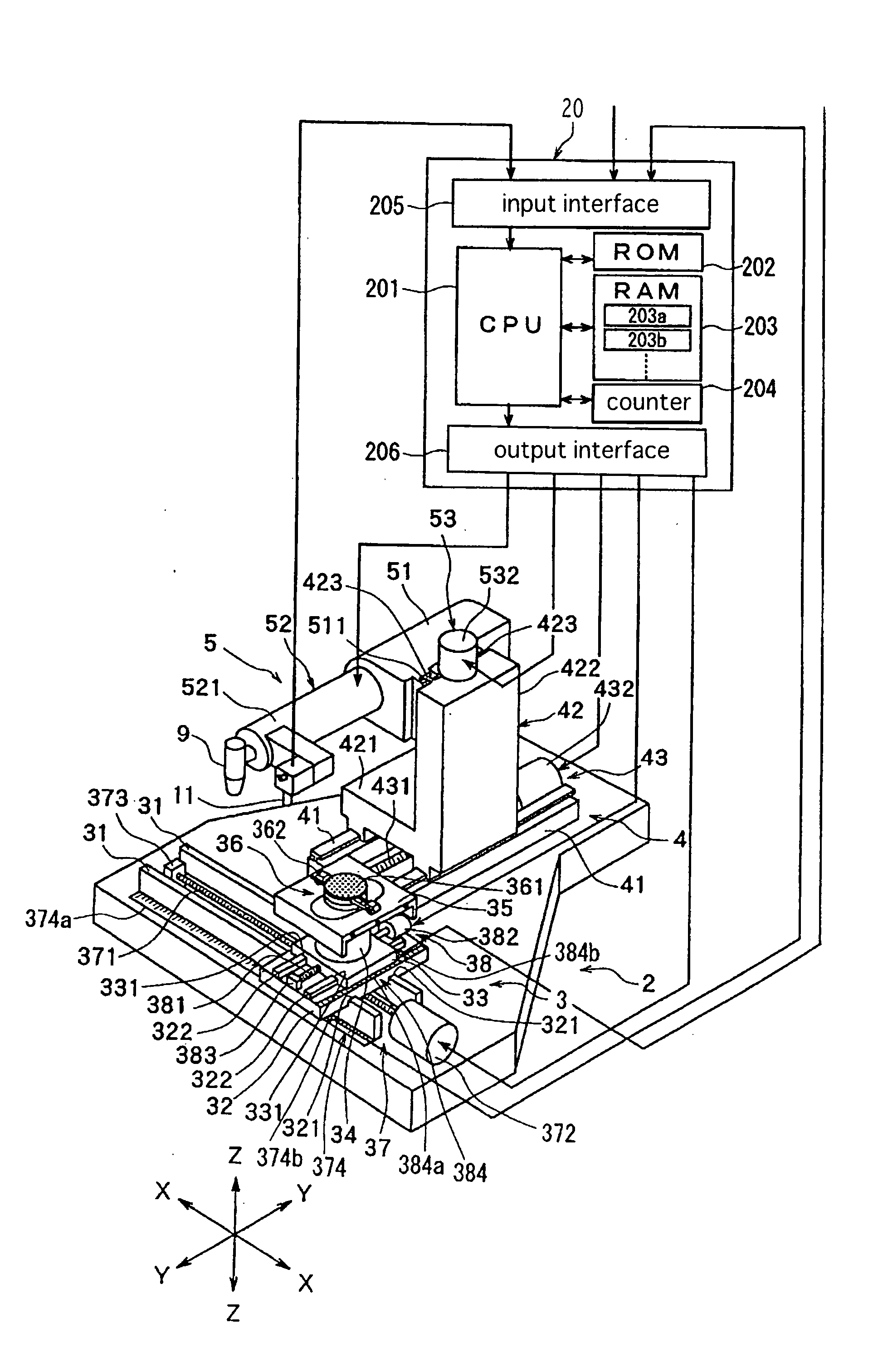
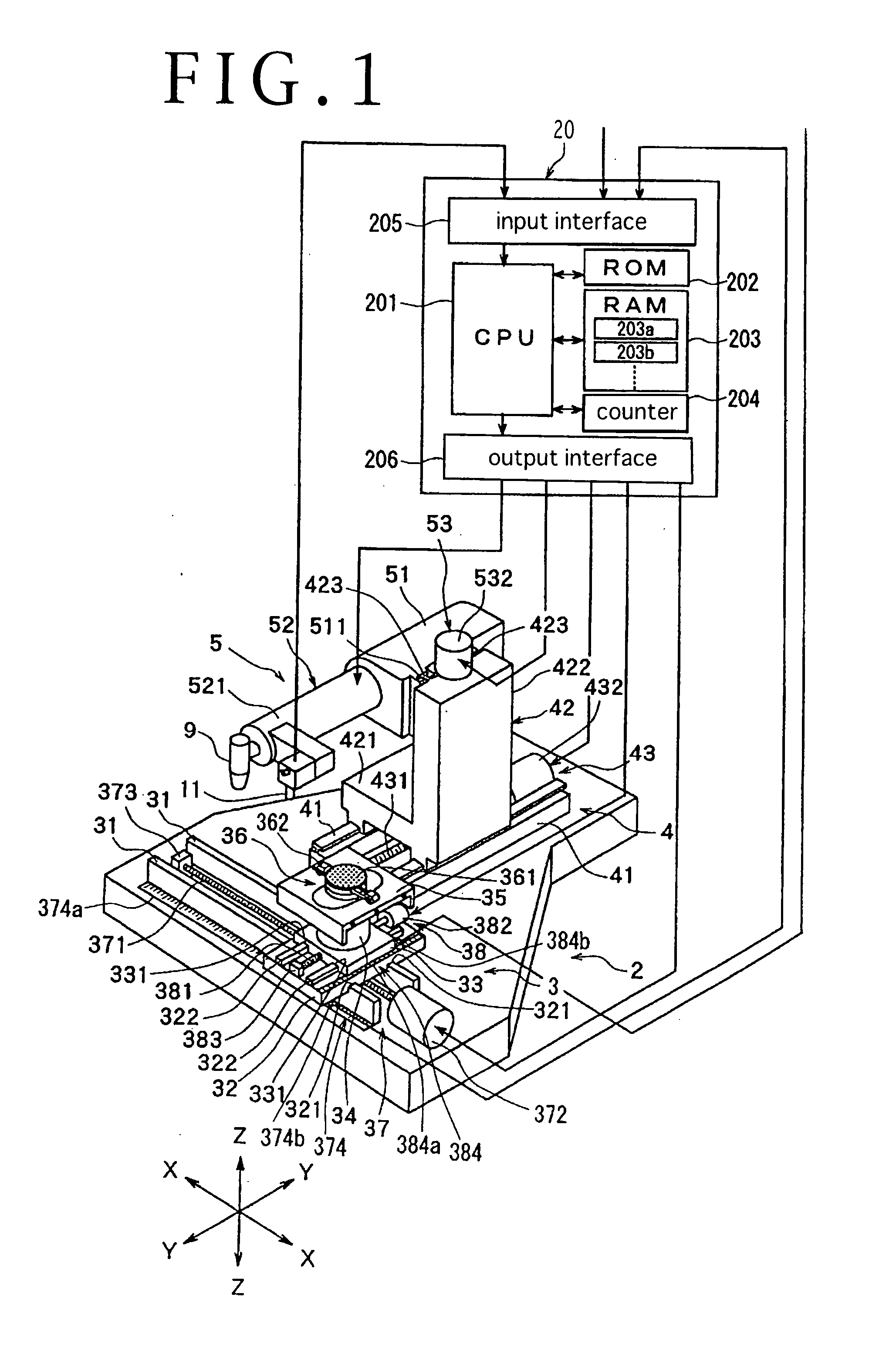
[0033] Now, preferred embodiments of the laser beam machining system configured according to the present invention will be described more in detail below, referring to the attached drawings. FIG. 1 shows a perspective view of the laser beam machining system configured according to the present invention. The laser beam machining system shown in FIG. 1 includes a stationary base 2, a chuck table mechanism 3 which is disposed on the stationary base 2 so as to be movable in a machining feed direction (X-axis direction) indicated by arrow X and which holds a work, a laser beam irradiation unit support mechanism 4 disposed on the stationary base 2 so as to be movable in an indexing feed direction (Y-axis direction) indicated by arrow Y orthogonal to the direction (X-axis direction) indicated by arrow X, and a laser beam irradiation unit 5 disposed on the laser beam irradiation unit support mechanism 4 so as to be movable in a direction (Z-axis direction) indicated by arrow Z.

[0034] The c...


PUM

PropertyMeasurementUnit
diametersaaaaaaaaaa
wavelengthaaaaaaaaaa
focal lengthaaaaaaaaaa

Abstract

A laser beam machining system including a chuck table for holding a work, and a laser beam irradiation unit for irradiating the work held on the chuck table with a laser beam, wherein the laser beam irradiation unit includes: a pulsed laser beam oscillator for oscillating a pulsed laser beam; a condenser for condensing the pulsed laser beam oscillated from the pulsed laser beam oscillator; a laser beam scanning unit disposed between the pulsed laser beam oscillator and the condenser and operative to deflect the pulsed laser beam to be inputted to the condenser; and a laser beam reshaping unit which ids disposed between the pulsed laser beam oscillator and the laser beam scanning unit and by which the energy distribution of the pulsed laser beam oscillated from the pulsed laser beam oscillator is reshaped into a top hat shape.

Description

BACKGROUND OF THE INVENTION [0001] 1. Field of the Invention [0002] The present invention relates to a laser beam machining system by which laser beam machining with a uniform depth can be applied to a work. [0003] 2. Description of the Related Art [0004] In the process of manufacturing a semiconductor device, a plurality of regions are demarcated by planned split lines called streets which are arranged in a lattice pattern on a face side of a roughly circular disk-like semiconductor wafer, and devices such as ICs and LSIs are formed respectively in the demarcated regions. Then, the semiconductor wafer is cut along the streets to split it into the regions provided with the devices, thereby producing individual semiconductor chips. In order to manufacture devices with smaller size and higher functions, a module structure has been put to practical use in which a plurality of semiconductor chips are stacked and bonding pads of the stacked semiconductor chips are connected to each other...

Claims


Application Information

Patent Timeline
Patent Type & Authority Applications(United States)
IPC IPC(8): B23K26/38B23K26/073
CPCB23K26/063B23K26/0656B23K26/386B23K26/0807B23K26/073B23K26/0622B23K26/066B23K26/082B23K26/389
Inventor NOMARU, KEIJI
Owner FUJITSU LTD
Why Eureka
Try Eureka