Liquid crystal display device

a technology of liquid crystal display and display screen, which is applied in the field of liquid crystal display screen, can solve the problems of unavoidable formation of spatial waste regions, difficulty in controlling the dimensions and shape of the periphery of the orientation film formed by inkjet printing, etc., and achieves the effect of facilitating the limitation of the application of the orientation film

Active Publication Date: 2008-03-13
PANASONIC LIQUID CRYSTAL DISPLAY CO LTD +1
View PDF33 Cites 25 Cited by
  • Summary
  • Abstract
  • Description
  • Claims
  • Application Information

AI Technical Summary

Benefits of technology

[0015]Further, the present invention controls as much as possible an increase in the manufacturing steps and limits application of the orientation film as far as the formation portion of the seal material in a structure where an orientation film is formed in proximity to a seal material in a liquid crystal display device.
[0016]According to the present invention, it becomes possible to obtain a liquid crystal display device where the formation region of the seal material and the orientation film are brought into proximity with each other and the display portion periphery is narrowly formed.
[0017]According to the present invention, it is possible to easily limit application of the orientation film in the formation region of the seal material, and it becomes possible to obtain a liquid crystal display device whose display region is wide in comparison to its peripheral portion by adding a half-exposure step or adjusting the viscosity of the orientation film.

Problems solved by technology

It has been pointed out that it is difficult to control the dimensions and shape of the periphery of an orientation film formed by the inkjet method.
Additionally, this spreading is not often uniform across the entire region around the resin film, and a spatially wasteful region is unavoidably formed.

Method used


Image

  • Liquid crystal display device
  • Liquid crystal display device
  • Liquid crystal display device

Examples


Embodiment Construction

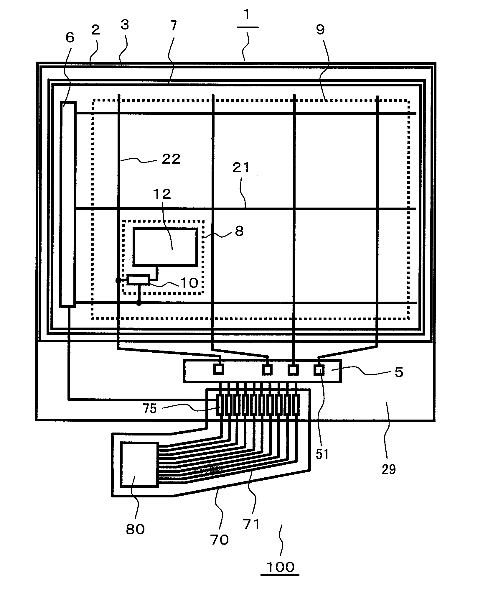
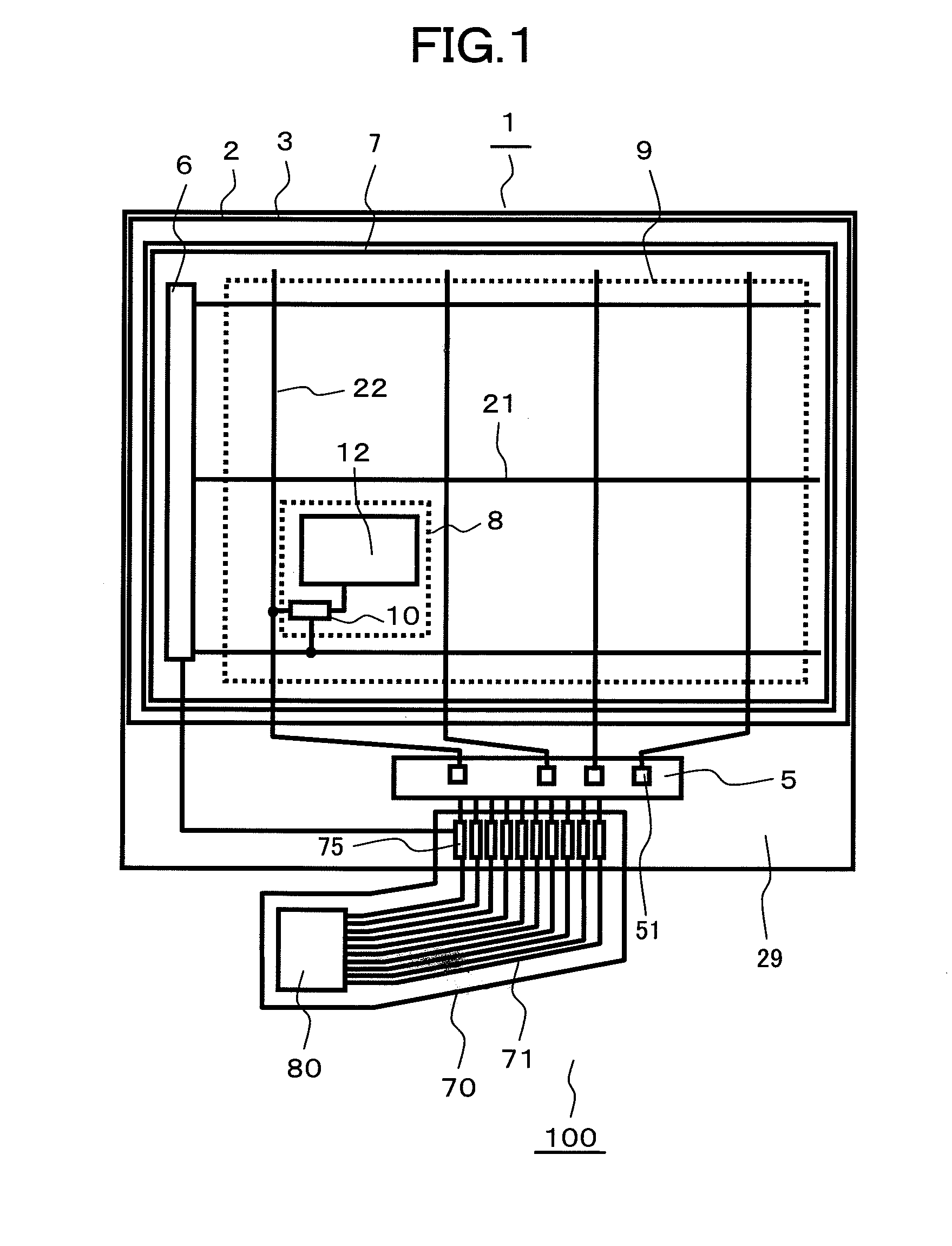
[0034]FIG. 1 is a plan diagram showing a liquid crystal display device 100 according to the present invention. The liquid crystal display device 100 is configured by a liquid crystal panel 1 and a control circuit 80. Signals and a power supply voltage needed for the display of the liquid crystal panel 1 are supplied from the control circuit 80. The control circuit 80 is mounted on a flexible substrate 70, and the signals are transmitted to the liquid crystal panel 1 via wires 71 and terminals 75.

[0035]Pixel electrodes 12 are disposed in pixel portions 8 of the liquid crystal panel 1. It will be noted that although the liquid crystal panel 1 is disposed with a large number of the pixel portions 8 in a matrix, just one pixel portion 8 is shown in FIG. 1 in order to avoid the drawing becoming complicated. The pixel portions 8 arranged in a matrix form a display region 9, with each of the pixel portions 8 fulfilling the role of a pixel of a display image, and display an image in the dis...


PUM

PropertyMeasurementUnit
distanceaaaaaaaaaa
affinityaaaaaaaaaa
transparent conductiveaaaaaaaaaa

Abstract

In a liquid crystal display device including an orientation film and a seal material, at a terminal connection portion where one substrate extends outward from another substrate, a step portion of an organic insulating film is formed on an inner side of the seal material to dispose a step, whereby spreading of the orientation film from the step portion to the seal material is limited. Lead wires that electrically interconnect connection terminals and pixel portions are formed on a portion of the organic insulating film where the film thickness is thin.

Description

BACKGROUND OF THE INVENTION[0001]1. Field of the Invention[0002]The present invention relates to a liquid crystal display device and in particular to technology effectively applied to a liquid crystal display device using an orientation film.[0003]2. Background Art[0004]In recent years, liquid crystal display devices have been heavily used as display devices. In particular, liquid crystal display devices have been used as display units in large televisions and portable devices because they are thin, lightweight, and low power consumption.[0005]However, liquid crystal display devices require an orientation film because they use a liquid crystal composition. Further, liquid crystal display devices have a structure where the liquid crystal composition is sealed between two substrates. For that reason, a seal material that seals the liquid crystal composition is disposed around the substrates. Further, the orientation film and the seal material are disposed in proximity to each other be...

Claims


Application Information

Patent Timeline
Patent Type & Authority Applications(United States)
IPC IPC(8): G02F1/1337G02F1/1335G02F1/1339
CPCG02F2201/50G02F1/1339
Inventor KOBAYASHI, SETSUOARAI, YOSHIHIRO
Owner PANASONIC LIQUID CRYSTAL DISPLAY CO LTD
Why Eureka
Try Eureka