Compact laser device

a laser device and compact technology, applied in semiconductor lasers, semiconductor/solid-state device testing/measurement, semiconductor/solid-state device details, etc., can solve the problem of limiting the available area, not helping to provide more than six mesas, and unsatisfactory production yield of laser chips per wafer to meet the quality targets of such laser devices with one mesa. problem, to achieve the effect of simplifying the marking of semiconductor chips

Active Publication Date: 2016-09-01
TRUMPF PHOTONIC COMPONENTS GMBH
View PDF12 Cites 0 Cited by
  • Summary
  • Abstract
  • Description
  • Claims
  • Application Information

AI Technical Summary

Benefits of technology

[0018]The method may enable an unambiguous marking of semiconductor chips or laser devices such that tracing of single, for example, laser devices is enabled. The tracing may be needed for quality management. Structuring of a functional layer like a metallization layer needed for, for example, electrically contacting avoids an additional manufacturing step like printing a serial number on top of the semiconductor chip. Marking of semiconductor chips may thus be simplified.

Problems solved by technology

Tests have shown that the production yield meaning the number of laser chips per wafer meeting the quality targets of such laser devices with one mesa is unsatisfactory.
Process steps like dicing and the like may require a minimum distance between a mesa and the edges of the semiconductor chip thus limiting the available area.
Surprisingly, it doesn't help to provide more than six mesas because the yield decreases again.

Method used


Image

  • Compact laser device
  • Compact laser device
  • Compact laser device

Examples


Embodiment Construction

[0034]Various embodiments of the invention will now be described by means of the Figures.

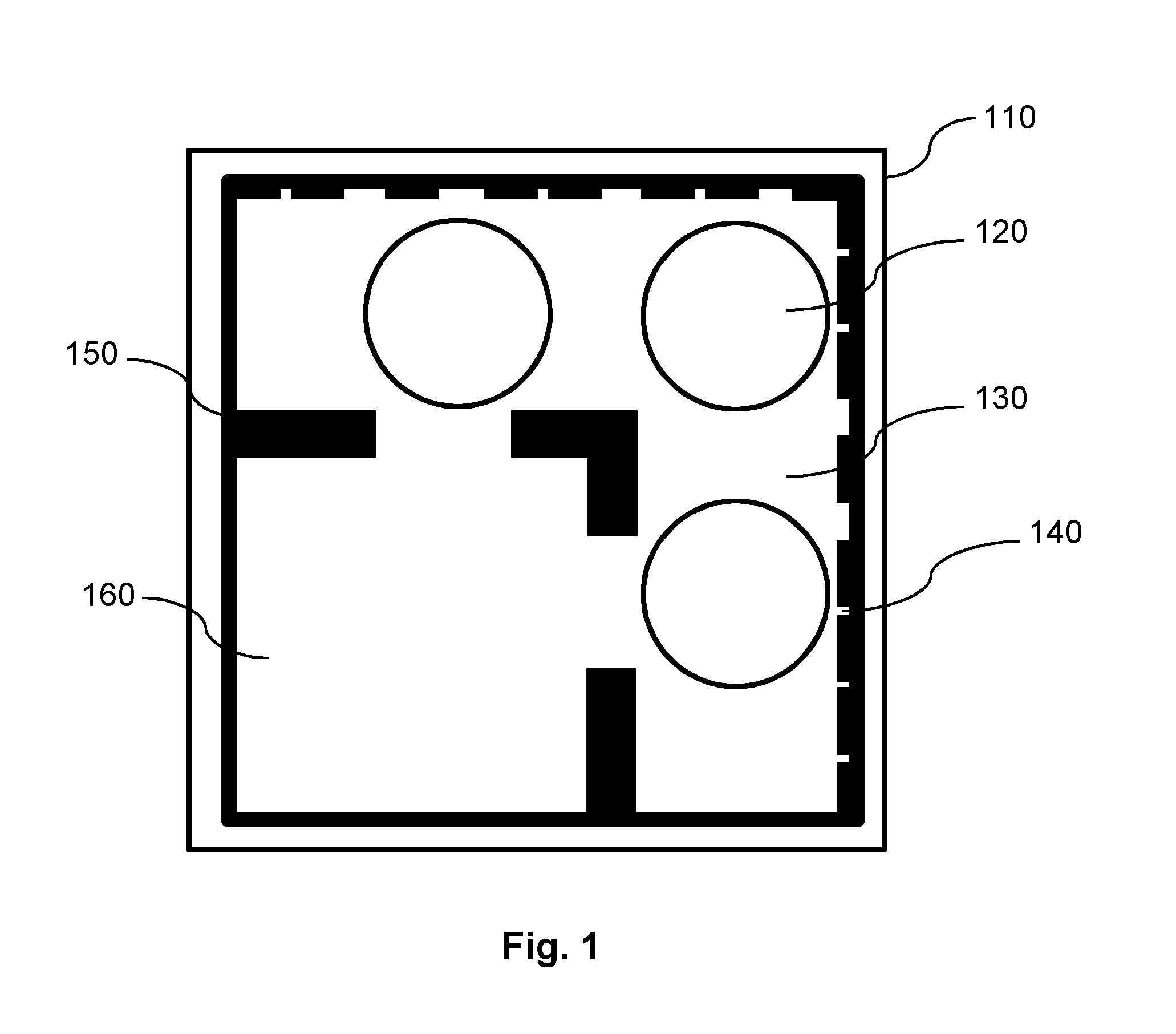
[0035]FIG. 1 shows a semiconductor ship 110 comprising three mesas 120. Each of the mesas comprises an optical resonator. A principal sketch of such an optical resonator is shown in FIG. 2. A metallization layer 130 is structured such that a bonding area 160 for electrically contacting the semiconductor chip 110 of the layer device is provided. Furthermore, alignment marks are provided in the metallization layer 130 for aligning the semiconductor chips 110 in the bonding process. The metallization layer 130 further comprises at the upper edge and the right edge a binary code 140 which comprises a number of extensions of different width. The extensions provide a binary code like a bar-code uniquely identifying each semiconductor chip 110. The binary code can be read out by means of optical inspection of the semiconductor chips 110.

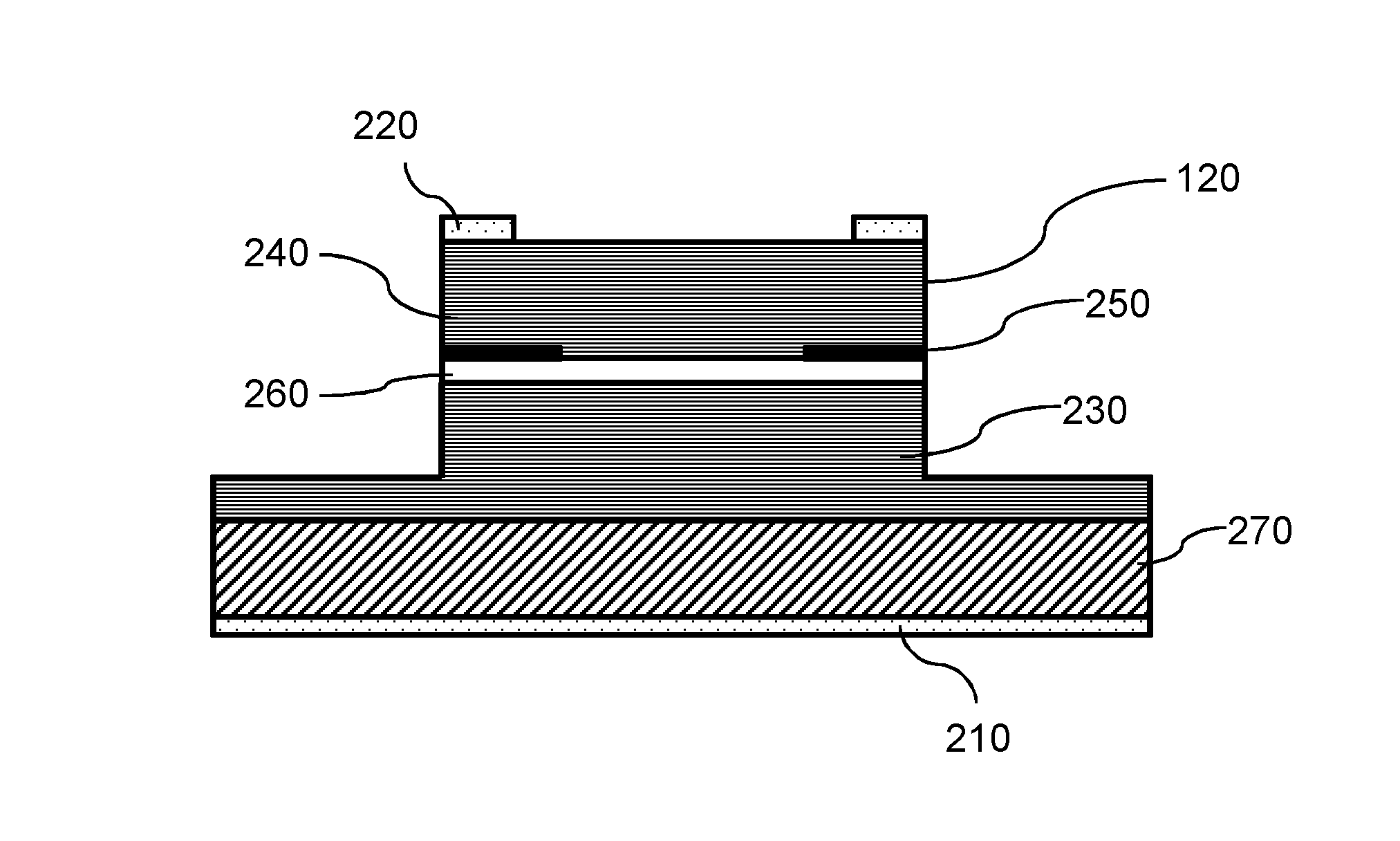
[0036]FIG. 2 shows a cross section of a VCSEL showing the optical ...


PUM


Abstract

The invention describes a laser device comprising between two and six mesas (120) provided on one semiconductor chip (110), wherein the mesas (120) are electrically connected in parallel such that the mesas (120) are adapted to emit laser light if a defined threshold voltage is provided to the mesas (120). Two to six mesas (120) with reduced active diameter in comparison to a laser device with one mesa improve the yield and performance despite of the fact that two to six mesas need more area on the semiconductor chip thus increasing the total size of the semiconductor chip (110). The invention further describes a method of marking semiconductor chips (110). A functional layer of the semiconductor chip (110) is provided and structured in a way that a single semiconductor chip (110) can be uniquely identified by means of optical detection of the structured functional layer. The structured layer enables identification of small semiconductor chips (110) with a size below 200 μm×200 μm.

Description

FIELD OF THE INVENTION[0001]The invention relates to a laser device wherein the laser device is especially suited for sensing applications. The invention further relates to a method of marking semiconductor chips in a unique way.BACKGROUND OF THE INVENTION[0002]Laser devices for optical sensors often comprise Vertically Cavity Surface Emitting Lasers (VCSEL). Next generation require an optical output power of at least 6 mW. State of the art VCSELs with such high output power are realized by increasing the diameter of the aperture or active diameter of the VCSELs (˜14 um). At the same time the total die size needs to be as small as possible and yield of the laser device has to be high in order to meet the cost targets.SUMMARY OF THE INVENTION[0003]It's thus an object of the present invention to provide an improved laser device enabling a combination of a small die or chip size and high yield.[0004]According to a first aspect a laser device comprising between two and six mesas provide...

Claims


Application Information

Patent Timeline
Patent Type & Authority Applications(United States)
IPC IPC(8): H01S5/028H01L31/16H01S5/22H01S5/183H01S5/042H01S5/42
CPCH01S5/028H01S5/042H01L31/16H01S5/22H01S5/18327H01S5/423H01L22/30H01L23/544H01L2223/54413H01L2223/54433H01L2223/5448H01L2924/0002H01L2924/00
Inventor GERLACH, PHILIPP HENNINGWEIGL, ALEXANDER
Owner TRUMPF PHOTONIC COMPONENTS GMBH
Why Eureka
Try Eureka