Insulated gate power semiconductor device and method for manufacturing such a device

Active Publication Date: 2019-04-25
HITACHI ENERGY SWITZERLAND AG
View PDF0 Cites 2 Cited by
  • Summary
  • Abstract
  • Description
  • Claims
  • Application Information

AI Technical Summary

Benefits of technology

[0028]Furthermore, the inventive device can be manufactured without adding delicate manufacturing steps. It is a simple, cheap and fast manufactu

Problems solved by technology

However, such a prior art device having a highly doped enhancement layer 95 will suffer from worse SOA and breakdown voltage compared to standard trench IGBTs.
Practical enhancement layer doping concentrations are therefore limited to values smaller than 2.5*1016 cm−3 to prevent excessive electric fields and therefore degradation of the blocking performance and turn-off SOA.
Nevertheless, the introduction of p doped protection pillows 8 at the trench bottoms 76 improves the device robustness, being able to postpone the onset of the breakdown mechanism, but is not able to redeem the inherent weakness of a trench IGBT device sufficiently where the impact ionization is caused by increased enhancement do

Method used


Image

  • Insulated gate power semiconductor device and method for manufacturing such a device
  • Insulated gate power semiconductor device and method for manufacturing such a device
  • Insulated gate power semiconductor device and method for manufacturing such a device

Examples


Example

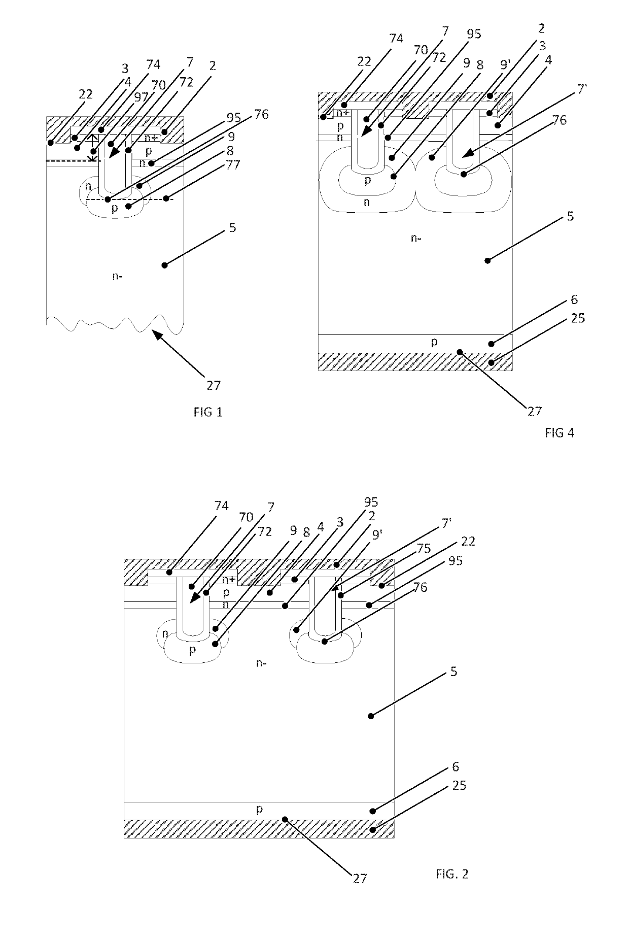
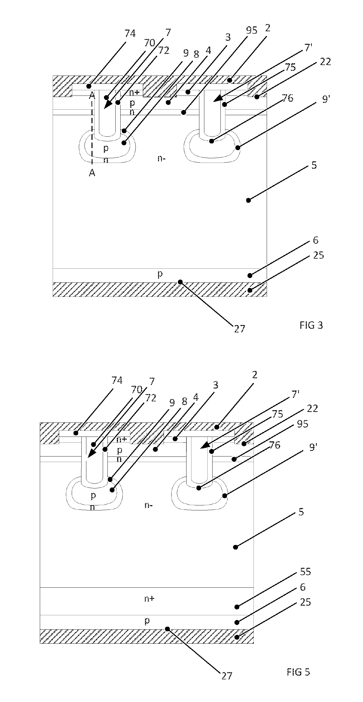
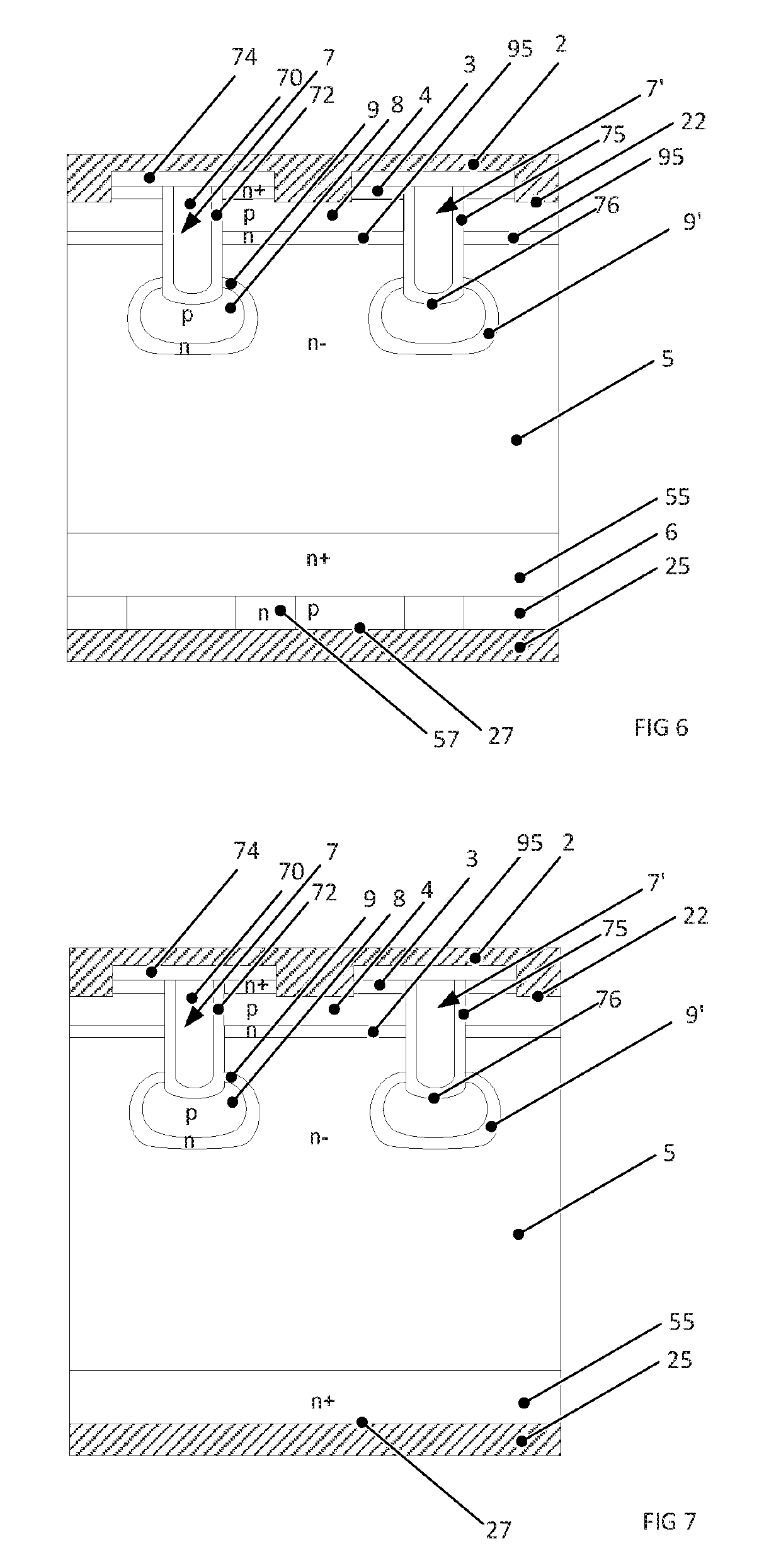
[0047]In FIG. 1 a structure on an emitter side 22 for an inventive insulated gate power semiconductor device is shown. The device comprises an emitter electrode 2 on an emitter side 22 and a collector electrode 25 on a collector side 27, which collector side 27 is arranged opposite to the emitter side 22. An (n−) doped drift layer 5 is arranged between the emitter side 22 and the collector side 27. A p doped base layer 4 is arranged between the drift layer 5 and the emitter side 22. The base layer 4 contacts the emitter electrode 2. An n doped source layer 3 having higher doping concentration than the drift layer is also arranged on the emitter side 22. The source layer 3, which is separated from the drift layer 5 by the base layer 4, contacts the emitter electrode 2. The source layer 3 may be arranged such that the source layer 3 is arranged at both sides of each gate electrode 7, 7′.

[0048]The doping concentration of the base layer 4 and the drift layer 5 can be freely chosen due t...


PUM


Abstract

An insulated gate power semiconductor device includes an (n−) doped drift layer between an emitter side and a collector side. A p doped protection pillow covers a trench bottom of a trench gate electrode. An n doped enhancement layer having a maximum enhancement layer doping concentration in an enhancement layer depth separates the base layer from the drift layer. An n doped plasma enhancement layer having a maximum plasma enhancement layer doping concentration covers an edge region between the protection pillow and the trench gate electrode. The n doping concentration decreases from the maximum enhancement layer doping concentration towards the plasma enhancement layer and the n doping concentration decreases from the maximum plasma enhancement layer doping concentration towards the enhancement layer such that the n doping concentration has a local doping concentration minimum between the enhancement layer and the plasma enhancement layer.

Description

TECHNICAL FIELD[0001]The invention relates to the field of power electronics, and more particularly to a device as such according to the preamble of the independent claim 1 or to a method for manufacturing an insulated gate power semiconductor device according to the independent claim 12.BACKGROUND ART[0002]In FIG. 18 a prior art insulated gate bipolar transistor (IGBT) is shown as known from EP 0 795 911 A2. The prior art device comprises an active cell with layers of different conductivity types in the following order between an emitter electrode 2 on an emitter side 22 and a collector electrode 25 on a collector side 27 opposite to the emitter side 22: an (n+) doped source layer 3, a p doped base layer 4, which contacts the emitter electrode 2, an n doped enhancement layer 95, an (n−) doped drift layer 5, an (n+) doped buffer layer 55 and a p doped collector layer 6.[0003]A trench gate electrode 7 is arranged on the emitter side 22, which comprises a gate layer 70 and a first ele...

Claims


Application Information

Patent Timeline
IPC IPC(8): H01L29/66H01L29/739H01L29/78H01L29/06H01L29/10
CPCH01L29/66734H01L29/7397H01L29/7813H01L29/66348H01L29/0619H01L29/10H01L21/26513H01L21/266H01L21/2253H01L29/0623H01L29/0834
Inventor DE-MICHIELIS, LUCACORVASCE, CHIARA
Owner HITACHI ENERGY SWITZERLAND AG
Why Eureka
Try Eureka