

Wafer processing method and wafer processing apparatus
- Summary
- Abstract
- Description
- Claims
- Application Information
AI Technical Summary
Benefits of technology
Problems solved by technology
Method used
Image

Examples
first embodiment
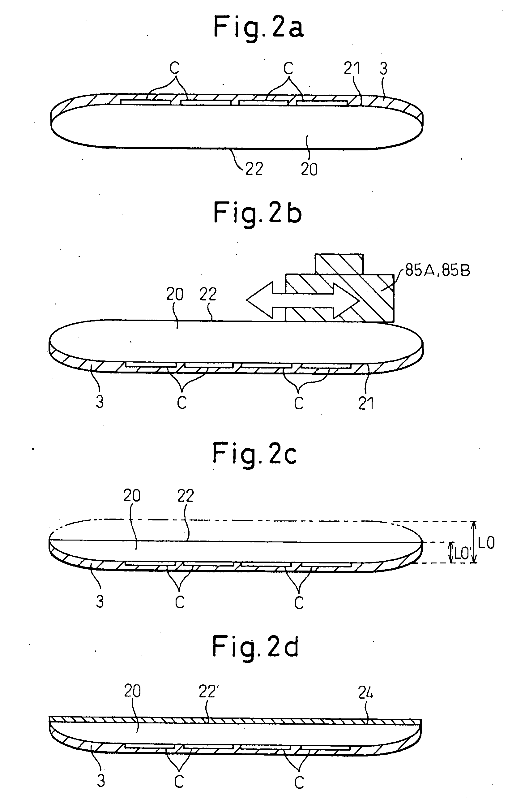
[0052]FIG. 3 is a schematic diagram of the die attachment paste application unit according to the present invention. The die attachment paste application unit 30 shown in FIG. 3 is a spin-coat type application unit 30A. Note that the surface protection film 3 and the circuit patterns C have been omitted from FIGS. 3, 4 and 8.
[0053] In the embodiment shown in FIG. 3, the die attachment paste application unit 30 comprises a holding table 33 that can be rotated by a motor 34, and a dispenser 32 that dispenses die attachment paste.
[0054] When the wafer 20 is held on the table 33 with its back surface 22 facing upward, a predefined amount of the die attachment paste is dispensed from the dispenser 32 onto the back surface 22 of the wafer 20. Next, when the table 33 is rotated about its central axis by the motor 34, the die attachment paste is scattered radially by centrifugal force toward the peripheral surface of the housing 31. The die attachment paste film 24 is thereby formed on the...
second embodiment
[0057]FIG. 4 is a schematic diagram of the die attachment paste application unit according to the present invention. The die attachment paste application unit 30 shown in FIG. 4 is a screen-printing type application unit 30B.
[0058] As shown in FIG. 4, the movable squeegee 42 is arranged inside the frame body 41 so as to move along the inner walls of the frame body 41. Moreover, the screen 44 having a hole 45 of a shape corresponding to the wafer 20, is provided on the lower surface of the frame body 41.
[0059]FIGS. 5a to 5c are views for explaining the die attachment paste application unit according to the second embodiment of the present invention. First, as shown in FIG. 5a, with its back surface 22 facing upward, the wafer 20 is held on the table 43, and the squeegee 42 is placed on one side in the frame body 41. Next, a predetermined amount of the die attachment paste 49 is supplied to one side of the squeegee 42, directed to the direction of movement of the squeegee 42.
[0060] ...
PUM
| Property | Measurement | Unit |
|---|---|---|
| Current | aaaaa | aaaaa |
| Digital information | aaaaa | aaaaa |
| Time | aaaaa | aaaaa |
Abstract
Description
Claims
Application Information