Stacked multi-chip package with EMI shielding

a technology of stacked multi-chip packages and shielding, which is applied in the direction of semiconductor devices, semiconductor/solid-state device details, electrical apparatus, etc., can solve the problems of inability to physically separate sensitive equipment and sources of electromagnetic radiation, inability to decouple only partially, and large space occupation of metal cans of this type on the substrate surfa

Active Publication Date: 2008-03-20
HONG KONG APPLIED SCI & TECH RES INST
View PDF12 Cites 42 Cited by
  • Summary
  • Abstract
  • Description
  • Claims
  • Application Information

AI Technical Summary

Problems solved by technology

Within such packages physical separation of sensitive equipment and sources of electromagnetic radiation is not practical and decoupling is only partially effective.
However, metal cans of this type take up considerable space on the substrate surface and tended to be not very robust often dislodging from the substrate surface due to cyclic stress loading on the solder joints holding the can to the substrate.
They also present an obstacle to the flow of molding epoxy and water vapor may accumulate within the can if the electrical equipment experiences a sudden change in environmental conditions.

Method used


Image

  • Stacked multi-chip package with EMI shielding
  • Stacked multi-chip package with EMI shielding
  • Stacked multi-chip package with EMI shielding

Examples


Embodiment Construction

[0024]In the specification and claims 1 mil=25.4 micrometer (1×10⁻⁶ m).

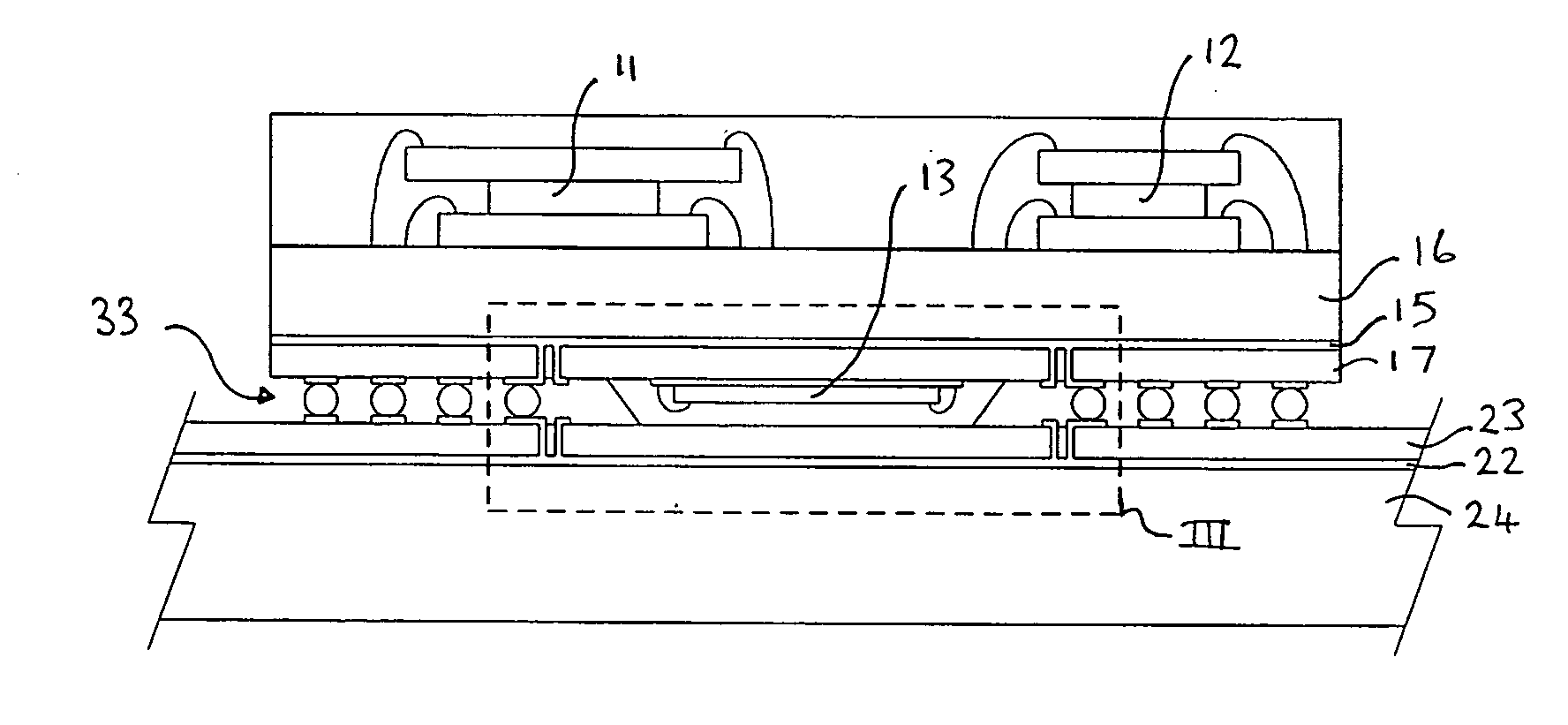
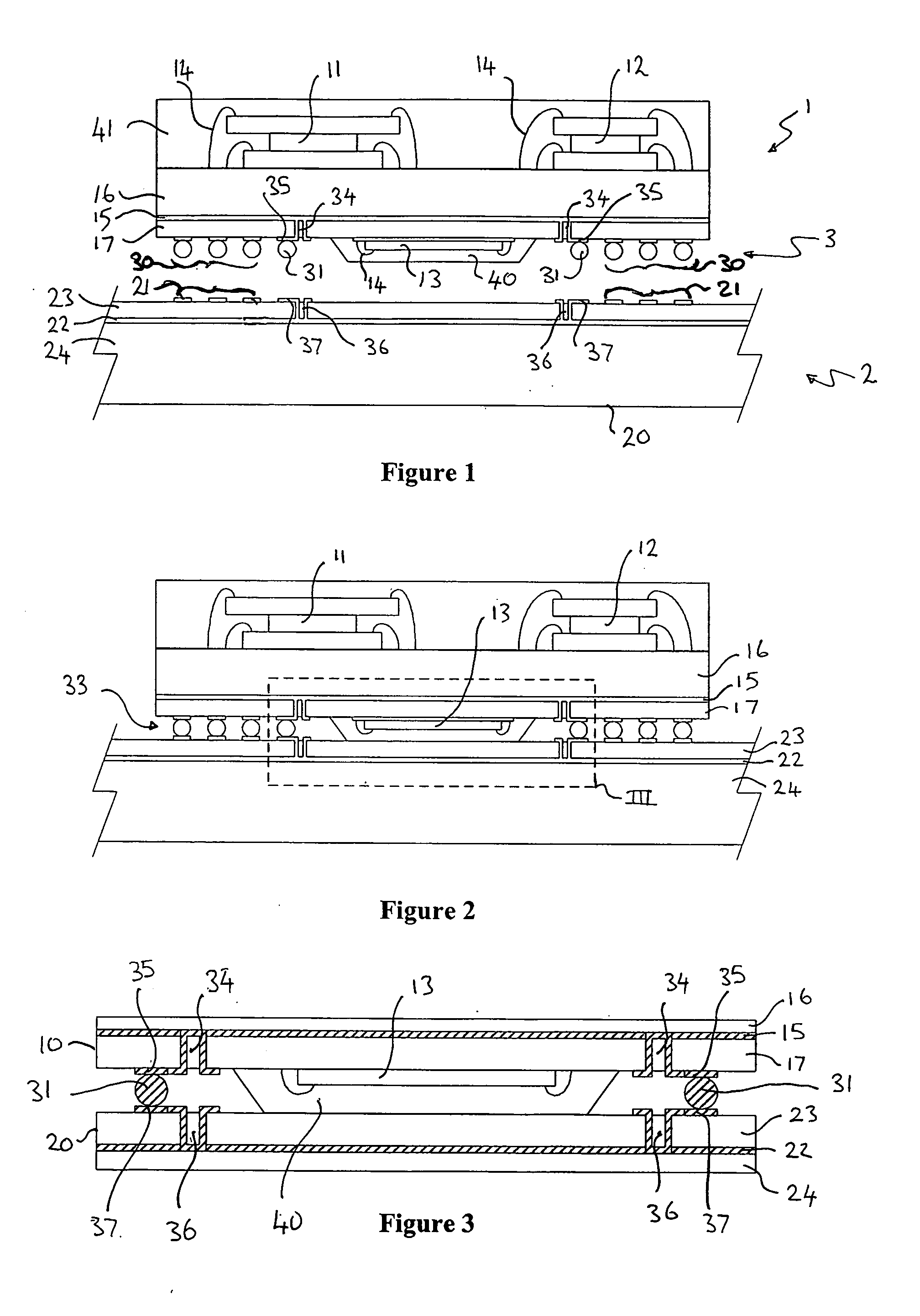
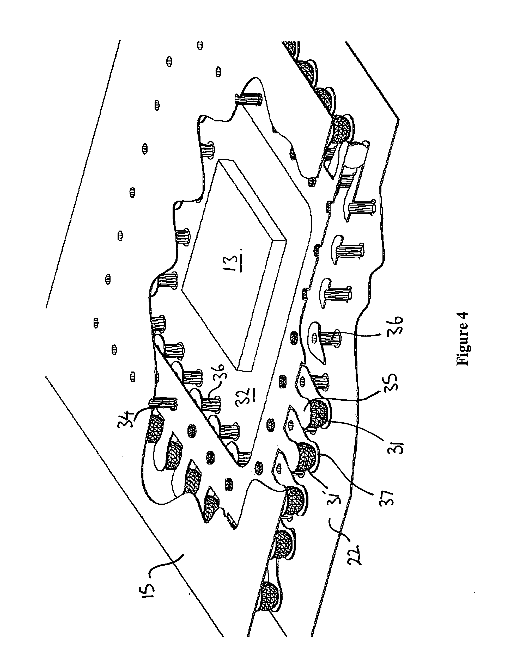
[0025]Generally the invention is a stacked multi-chip package with first and second substrates mounted together by a grid array of metallic connecting nodes, such as a solder Ball Grid Array. Each substrate has a ground plane laminated between dielectric layers of the substrate. A sensitive or EMI generating component is mounted between the first and second substrates and is surrounded by a group of the metallic connecting nodes that are also electrically connected to the ground planes of both substrates to form a conductive Faraday cage about the component.

[0026]In the drawings there is depicted an exemplary embodiment of the invention as practiced in a multi-chip integrated package having both radio frequency (RF) and digital integrated circuit (IC) chips packaged together in a stacked substrate arrangement. This type of arrangement is often termed a stacked multi-chip module (MCM). This exemplary example is no...


PUM


Abstract

A stacked multi-chip package with an EMI shielded component has first and second substrates mounted together by a grid array of metallic connecting nodes, such as a solder Ball Grid Array. Each substrate has a conductive plane associated with it. An electronic component is mounted between the first and second substrates and is surrounded by a group of the metallic connecting nodes that are also electrically connected to the conductive planes of both substrates to form a conductive Faraday cage about the component.

Description

BACKGROUND TO THE INVENTION[0001]1. Field of the Invention[0002]The Invention relates to multi-chip packages and in particular to stacked multi-chip packages. More particularly, the invention relates to a stacked multi-chip package with EMI shielding to isolate a chip in the package from electromagnetic interference, or from causing electromagnetic interference, in other parts of the package.[0003]2. Background Information[0004]Electromagnetic interference (EMI), also known as radio frequency interference (RFI), is caused by electromagnetic radiation and is a significant consideration in electronic circuit design. Electromagnetic radiation is emitted by electronic circuits and components carrying changing electrical signals. There are three main techniques for ameliorating or eliminating EMI. The first technique is to physically separate sensitive components from the source of any electromagnetic radiation. The second technique is to use bypass or decoupling capacitors and filters t...

Claims


Application Information

Patent Timeline
Patent Type & Authority Applications(United States)
IPC IPC(8): H01L23/02H01L21/00
CPCH01L23/5385H01L23/552H01L2924/15321H01L2224/73265H01L2224/32225H01L2224/32145H01L24/48H01L2924/3025H01L2924/19041H01L2924/1532H01L2924/15311H01L2224/48227H01L2224/48091H01L25/0652H01L2924/00014H01L2924/00012H01L2924/00H01L24/73H01L2924/14H01L2924/181H01L2224/45099H01L2224/45015H01L2924/207
Inventor LEUNG, LAP WAICHEN, YU-CHIHSHAM, MAN-LUNGCHUNG, CHANG-HWA
Owner HONG KONG APPLIED SCI & TECH RES INST
Why Eureka
Try Eureka