Semiconductor device and method of forming the same

a technology of semiconductor devices and semiconductors, applied in the direction of semiconductor devices, basic electric elements, electrical appliances, etc., can solve the problems of deteriorating the retention and writing characteristics of dram memory cells, and reducing the channel length, so as to prevent any unnecessary parasitic capacitance, and suppress the threshold voltage variation

Inactive Publication Date: 2008-03-27
ELPIDA MEMORY INC
View PDF6 Cites 25 Cited by
  • Summary
  • Abstract
  • Description
  • Claims
  • Application Information

AI Technical Summary

Benefits of technology

[0025]It is another object of the present invention to provide a semiconductor device including one or more trench gate transistors with a groove or grooves that increase the channel length, without increasing parasitic capacitance.
[0046]The method may further include carrying out a baking process in a hydrogen atmosphere after the separate grooves are formed. The semiconductor substrate may typically be a silicon substrate. The baking process may be carried out to cause silicon atoms to move, thereby reducing surface-irregularly on the opening edge of each separate groove. Carrying out the baking process in the hydrogen atmosphere can prevent the above-described problems with the residue.

Problems solved by technology

Reduction of the channel length of a transfer gate transistor performing as a memory cell switching transistor can deteriorate the performances thereof.
Deterioration of the performance of the transfer gate transistor can deteriorate retention and writing characteristics of DRAM memory cells.
The DRAM having the trench gate transistors may have parasitic capacitance that need increased current to writing operation, thereby increasing the power consumption.
The parasitic capacitances coupled to the word line can cause a delay of signal transmission through the word line.
The residual portion of the conductive film in the void may cause a short circuit formation between adjacent word lines.

Method used


Image

  • Semiconductor device and method of forming the same
  • Semiconductor device and method of forming the same
  • Semiconductor device and method of forming the same

Examples


Embodiment Construction

[0067]Selected embodiments of the present invention will now be described with reference to the drawings. It will be apparent to those skilled in the art from this disclosure that the following descriptions of the embodiments of the present invention are provided for illustration only and not for the purpose of limiting the invention as defined by the appended claims and their equivalents.

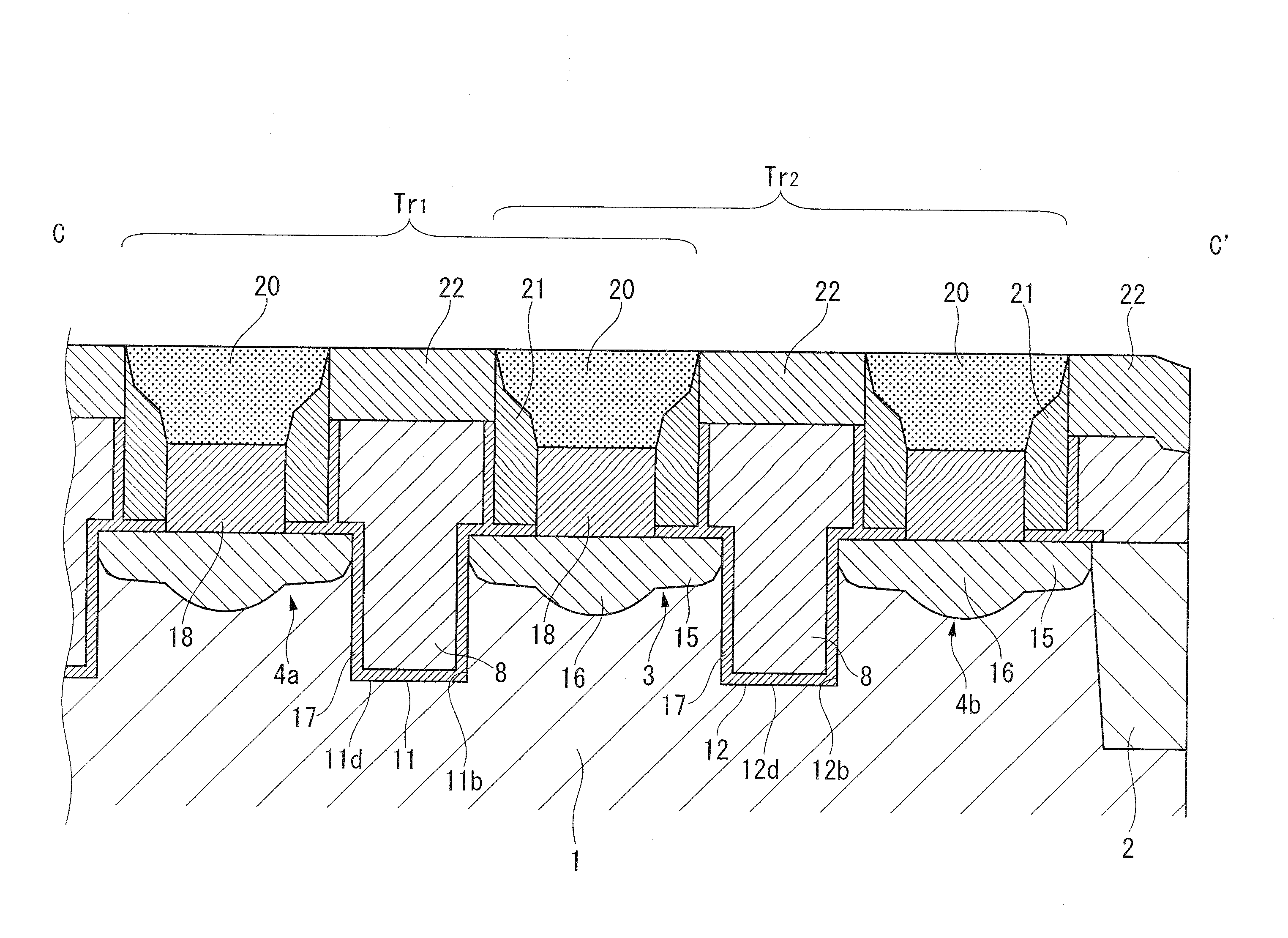
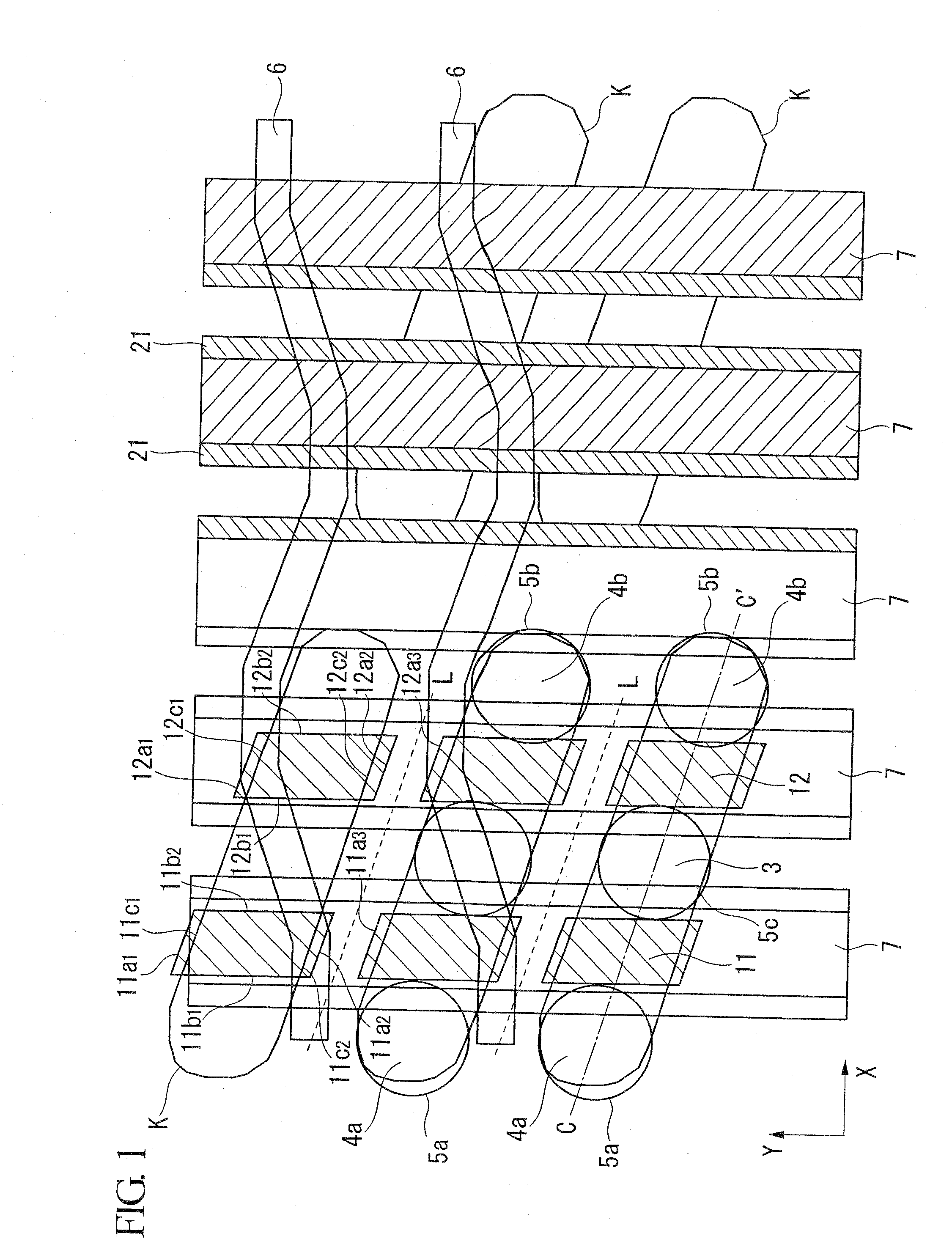
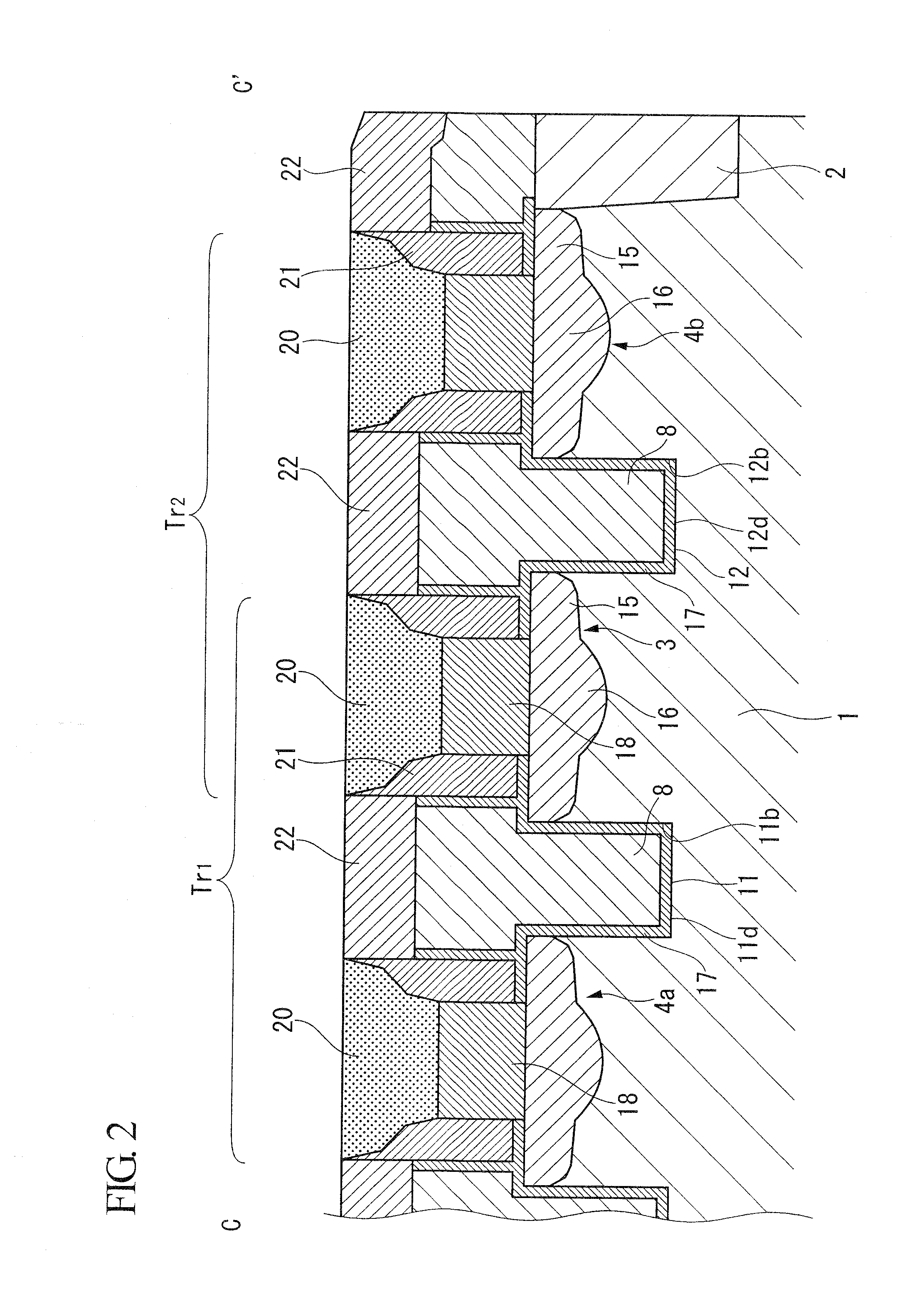
[0068]FIG. 1 is a fragmentary plan view illustrating a semiconductor device in accordance with a first embodiment of the present invention. FIG. 2 is a fragmentary cross sectional elevation view illustrating the semiconductor device, taken along a C-C′ line of FIG. 1.

[0069]The semiconductor device includes a semiconductor substrate 1, which may be made of a semiconductor such as silicon, having a predetermined impurity concentration. A trench isolation film 2 is electively formed in the surface of the semiconductor substrate 1. The trench isolation film 2 can be formed by shallow trench isolation m...


PUM


Abstract

A semiconductor device and a method of forming the semiconductor device are provided. The semiconductor device may include, but is not limited to, a semiconductor substrate and a third array of semiconductor elements. The semiconductor substrate may include a first array of separate grooves, a second array of separate active regions, and at least an isolating region, the isolating region separating the separate active regions from each other. Each separate groove extends in the separate active region and does not extend over the isolating region. The third array of semiconductor elements is provided on the semiconductor substrate. Each of the semiconductor elements has an electrically conductive portion that is provided in the separate groove. The semiconductor element may be a trench gate transistor, and the electrically conductive portion may be a gate electrode.

Description

BACKGROUND OF THE INVENTION[0001]1. Field of the Invention[0002]The present invention generally relates to a semiconductor device and a method of forming the same. More specifically, the present invention relates to a semiconductor device including a trench gate transistor, and a method of forming the same.[0003]Priority is claimed on Japanese Patent Application No. 2006-255746, filed Sep. 21, 2006, the content of which is incorporated herein by reference.[0004]2. Description of the Related Art[0005]All patents, patent applications, patent publications, scientific articles, and the like, which will hereinafter be cited or identified in the present application, will hereby be incorporated by reference in their entirety in order to describe more fully the state of the art to which the present invention pertains.[0006]A semiconductor memory device such as a dynamic random access memory (DRAM) includes a plurality of memory cells. Each memory cell includes a switching transistor and a c...

Claims


Application Information

Patent Timeline
Patent Type & Authority Applications(United States)
IPC IPC(8): H01L29/78H01L21/336
CPCH01L21/823437H01L27/10855H01L27/10873H01L29/7834H01L29/4236H01L29/66621H01L27/10888H10B12/0335H10B12/05H10B12/485
Inventor AISO, FUMIKI
Owner ELPIDA MEMORY INC
Why Eureka
Try Eureka