Electromagnetic shielding using through-silicon vias

a technology of silicon vias and electromagnetic shielding, which is applied in the direction of semiconductor devices, semiconductor/solid-state device details, electrical apparatus, etc., can solve the problems of high noise coupling between the integrated circuit and the analog circuit, limiting the performance of the analog circuit, and easy to affect the noise generated in the analog circuit. achieve the effect of better electromagnetic isolation

Active Publication Date: 2008-03-27
TAIWAN SEMICON MFG CO LTD
View PDF4 Cites 150 Cited by
  • Summary
  • Abstract
  • Description
  • Claims
  • Application Information

AI Technical Summary

Benefits of technology

[0009]Since through-silicon vias extend all the way from the top surface of the substra

Problems solved by technology

The high degree of integration causes high noise coupling between the integrated circuits.
Particularly, analog circuits are easily affected by the noise generated in digital circuits.
This significantly limits the performance of analog circuits, such as analog to digital converters that are extremely sensitive

Method used


Image

  • Electromagnetic shielding using through-silicon vias
  • Electromagnetic shielding using through-silicon vias
  • Electromagnetic shielding using through-silicon vias

Examples


first embodiment

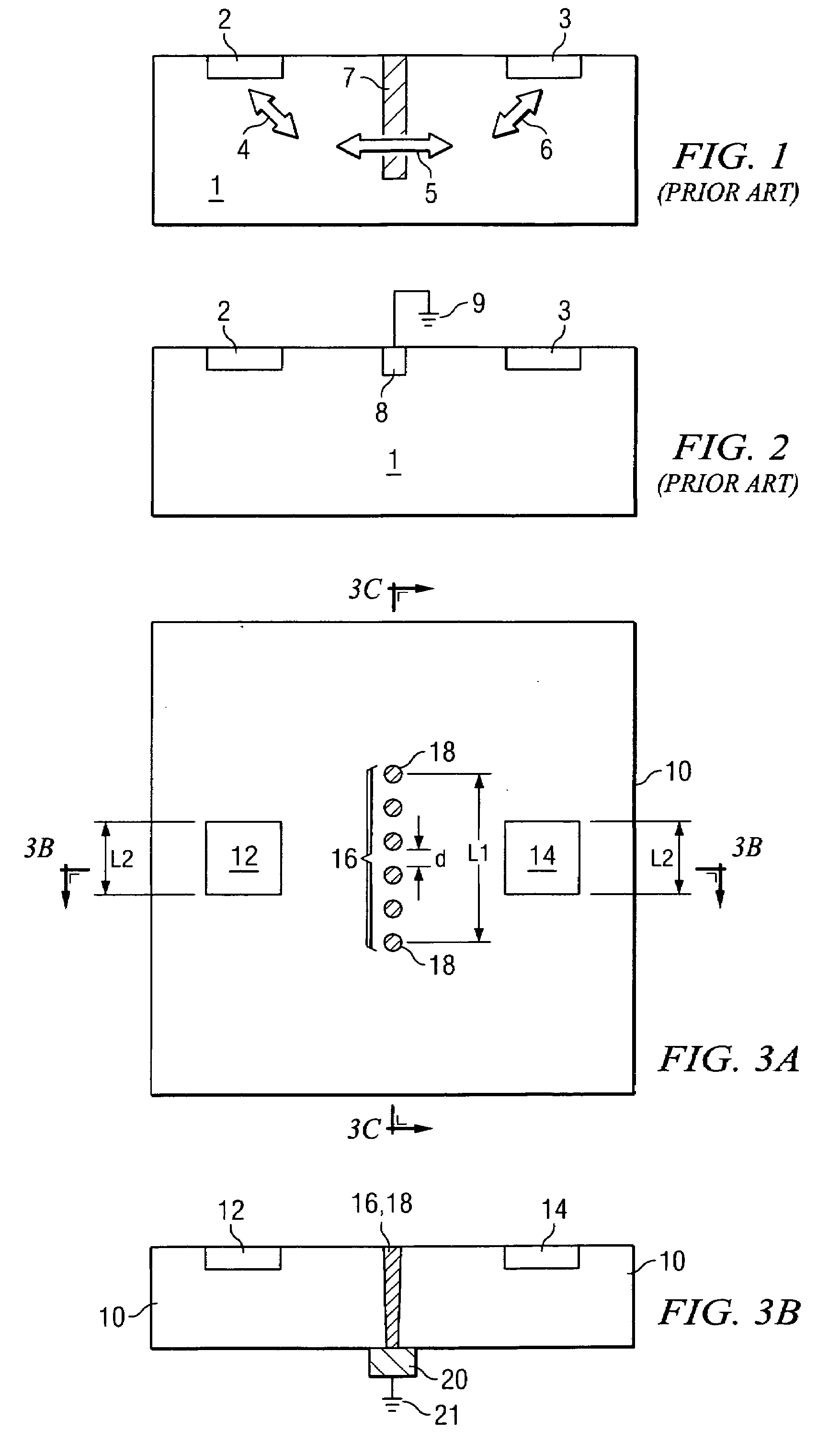
[0024]FIG. 3A illustrates a top view of the present invention. A semiconductor substrate 10 includes a first circuit region 12 and a second circuit region 14, wherein at least one of the circuit regions 12 and 14 includes devices that are sensitive to electromagnetic (EM) noise. Regions 12 and 14 are thus preferably isolated from each other. In the preferred embodiment, one of the circuit regions 12 and 14 is an analog region, while the other is a digital region. Alternatively, circuit regions 12 and 14 are either both analog regions, both digital regions, or compound regions that include both analog and digital circuits.

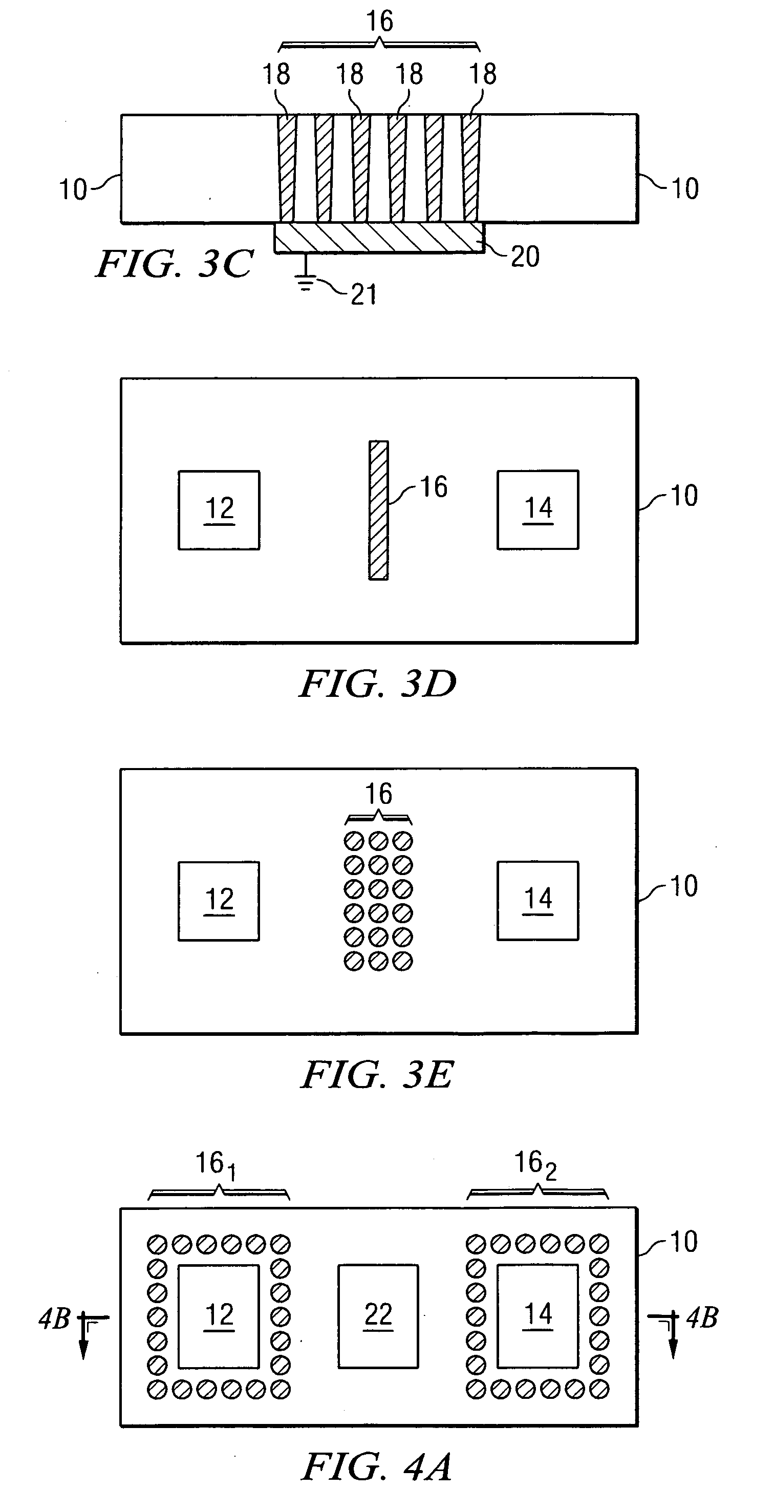
[0025]An EM isolation structure 16 is formed in substrate 10 in a direct path between circuit regions 12 and 14. In the preferred embodiment, EM isolation structure 16 comprises at least one through-silicon via 18, also sometimes referred to as a through-wafer via or a through-substrate via in the art. Through-silicon vias are vias that extend from the top surface o...

second embodiment

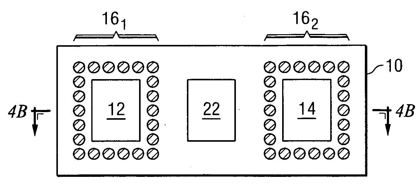
[0030]FIGS. 4A through 4D illustrate a Referring to FIG. 4A, EM isolation structure 16 includes an EM isolation structure 161 encircling circuit region 12. To achieve better results, another EM isolation structure 162 may be formed to encircle circuit region 14. Furthermore, a circuit region 22 may be formed. Circuit region 22 is not encircled by any EM isolation structure. However, since the EM noise generated by circuit regions 12 and 14 is isolated by the respective isolation structures 161 and 162, circuit regions 12, 14 and 22 are still substantially protected from EM interference with each other.

[0031]FIG. 4B illustrates a cross-sectional view of the structure shown in FIG. 4A, wherein the cross-sectional view is taken along a line 4B-4B. Preferably, backside conductive layer 20 is formed and electrically connected to through-silicon vias 18 in isolation structures 161 and 162. Therefore, the EM interference from the sides and the bottom of circuit regions 12 and 14 are signi...


PUM


Abstract

An isolation structure for electromagnetic interference includes a semiconductor substrate, a first integrated circuit in the semiconductor substrate, a second integrated circuit in the semiconductor substrate, and an isolation structure in a direct path between the first and the second integrated circuits, wherein the isolation structure comprises a through-silicon via.

Description

TECHNICAL FIELD[0001]This invention relates generally to integrated circuits, and more particularly to the isolation of electromagnetic interference between integrated circuits.BACKGROUND[0002]Recent advances in IC design and fabrication make possible the integration of various types of integrated circuits, for example, digital and analog circuits on a same IC chip. The high degree of integration causes high noise coupling between the integrated circuits. Particularly, analog circuits are easily affected by the noise generated in digital circuits. This significantly limits the performance of analog circuits, such as analog to digital converters that are extremely sensitive to noise at the inputs. Besides the noise interference between digital circuits and analog circuits, noise interference also exists between digital circuit components. FIG. 1 illustrates a noise path between a digital circuit region 2 and an analog circuit region 3. Arrows 4, 5 and 6 symbolize one of the noise pat...

Claims


Application Information

Patent Timeline
IPC IPC(8): H01L29/00H01L21/331
CPCH01L21/76H01L21/823481H01L23/481H01L23/585H01L25/0657H01L2225/06513H01L2224/16146H01L2225/06541H01L2224/131H01L2225/06527H01L2224/13025H01L2924/014H01L2224/05009H01L2224/0557H01L2224/05568H01L2224/05001H01L2224/05124H01L2224/05147H01L2224/05166H01L2224/05181H01L2224/05184H01L24/05H01L2924/013H01L2924/00014
Inventor CHAO, CLINTONHSU, C.S.PENG, MARK SHANELU, SZU WEIKARTA, TJANDRA WINATA
Owner TAIWAN SEMICON MFG CO LTD
Why Eureka
Try Eureka