Organic substrate embedded package structure with integrated antenna and RF front end

A packaging structure, RF front-end technology, applied to antennas, semiconductor/solid-state device components, semiconductor devices, etc., can solve the problems of occupying the RF front-end module area, limiting the thickness of the antenna substrate, and packaging form limitations, and reducing the packaging area. , reduce parasitic effects, reduce the effect of package profile

Active Publication Date: 2022-07-29
INST OF MICROELECTRONICS CHINESE ACAD OF SCI
View PDF6 Cites 0 Cited by
  • Summary
  • Abstract
  • Description
  • Claims
  • Application Information

AI Technical Summary

Problems solved by technology

[0003] At present, the research on AiP mainly focuses on the integration of single-chip transceivers and antennas. However, the integration of multi-chip RF front-ends and antenna arrays faces the following technical problems: Most of the millimeter-wave chips used in RF front-ends are based on compound semiconductor technology. Surface transmission lines, inductance-capacitance air bridges, and back grounding requirements limit chip packaging to wire bonding, but as the operating frequency increases, the parasitic effects of bonding wires become more apparent; at the same time, electronic products require thinner and smaller packages. However, the light and thin packaging structure limits the thickness of the antenna substrate, thereby limiting the improvement of the antenna performance; in addition, when the antenna is integrated with the RF front-end, the gap between the active chip and the active chip, and between the antenna and the active chip The problem of electromagnetic interference is particularly serious; moreover, most of the passive components are surface-mounted on the motherboard, occupying the area of ​​the RF front-end module

Method used


Image

  • Organic substrate embedded package structure with integrated antenna and RF front end
  • Organic substrate embedded package structure with integrated antenna and RF front end
  • Organic substrate embedded package structure with integrated antenna and RF front end

Examples


Embodiment Construction

[0064] In order to make the objectives, technical solutions and advantages of the present invention more clearly understood, the present invention will be further described in detail below in conjunction with specific embodiments and with reference to the accompanying drawings.

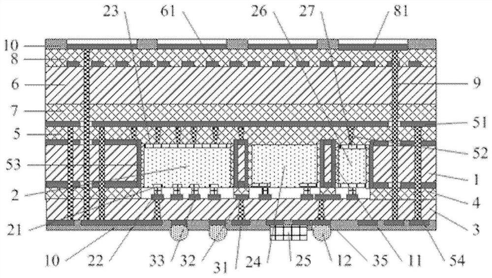
[0065] The invention discloses an organic substrate embedded packaging structure integrating an antenna and a radio frequency front end. Please refer to figure 1 , including: an antenna module; and a radio frequency front-end module, placed under the antenna module, the radio frequency front-end module includes: a No. 1 core board 1, the interior includes at least one through slot; The source surface, the other side surface is the back metal 23 of the active chip, the active chip 2 is embedded in the through groove of the No. 1 core board 1; the No. 1 dielectric layer 4 is placed under the No. 1 core board 1, A through slot is provided at a position corresponding to the through slot in the No. 1 core ...


PUM


Abstract

An organic substrate embedded packaging structure integrating an antenna and a radio frequency front end, comprising: an antenna module; and a radio frequency front end module placed under the antenna module, the radio frequency front end module comprising: a No. 1 core board, which includes at least one through slot inside ; At least one active chip, one side surface is an active surface, the other side surface is a back metal, the active chip is embedded in the through groove of the No. 1 core board; No. 1 dielectric layer, placed on No. 1 Below the core board, a through slot is provided at a position corresponding to the through slot in the No. 1 core board; The active side of the chip faces down, and is flip-mounted on the surface component pads of the No. 2 core board; the No. 2 dielectric layer is placed above the No. 1 core board, and a plurality of metallized blind holes are drilled inside. .

Description

technical field [0001] The invention relates to the technical field of semiconductor packaging, in particular to an organic substrate embedded packaging structure integrating a millimeter wave antenna and a radio frequency front end. Background technique [0002] In order to improve the integration level, the International Semiconductor Technology Development Route Organization proposes to surpass Moore's Law, aiming to integrate processors, memory, radio frequency modules, digital modules, analog modules, optoelectronic modules, sensing modules, etc. in a single package to achieve system-level packaging (System in Package, SiP), if the antenna is also integrated in a system-in-package, it is called an antenna-in-package (Antenna in Package, AiP). [0003] At present, the research on AiP mainly focuses on the integration of single-chip transceiver and antenna. However, the integration of multi-chip RF front-end and antenna array faces the following technical problems: the mi...

Claims


Application Information

Patent Timeline
Patent Type & Authority Patents(China)
IPC IPC(8): H01L25/18H01L23/488H01L23/552H01L23/66H01Q19/10
CPCH01L25/18H01L23/488H01L23/552H01L23/66H01Q19/10H01L2223/6677H01L2224/16225
Inventor 薛梅王启东曹立强宋阳
Owner INST OF MICROELECTRONICS CHINESE ACAD OF SCI
Why Eureka
Try Eureka