Electrical test probe and electrical test probe assembly

a technology of test probes and probe parts, applied in the direction of measurement devices, semiconductor/solid-state device testing/measurement, instruments, etc., can solve problems such as deformation or breakage, and achieve the effects of enhancing the abrasion resistance and ensuring the reliability of the probe tip portion

Active Publication Date: 2008-03-27
NIHON MICRONICS
View PDF3 Cites 18 Cited by
  • Summary
  • Abstract
  • Description
  • Claims
  • Application Information

AI Technical Summary

Benefits of technology

[0029]According to the first invention, since a probe tip reinforcement portion formed on a pedestal portion of a probe main body portion exerts a part of a reactive force of a bending force acting on a probe tip portion provided on the pedestal portion without preventing a tip of the probe tip portion from contacting an electrode as described above, it can reinforce the probe tip portion reliably.
[0030]According to the second invention, as a probe tip portion is in a multi-layer structure having a first highly hard metal material layer and a second metal material layer with excellent toughness, the features of both the metal material layers can be utilized effectively. Thus, it is possible to enhance abrasion resistance of the probe tip portion of the probe, prevent its defect or breakage, and improve durability of the probe.

Problems solved by technology

Also, as the fine probe tip portion protruded from the lower surface of the pedestal portion is made of the highly hard metal material, the fragility of the probe tip portion may cause defect or breakage when a load is applied to the tip of the probe tip portion.

Method used


Image

  • Electrical test probe and electrical test probe assembly
  • Electrical test probe and electrical test probe assembly
  • Electrical test probe and electrical test probe assembly

Examples


Embodiment Construction

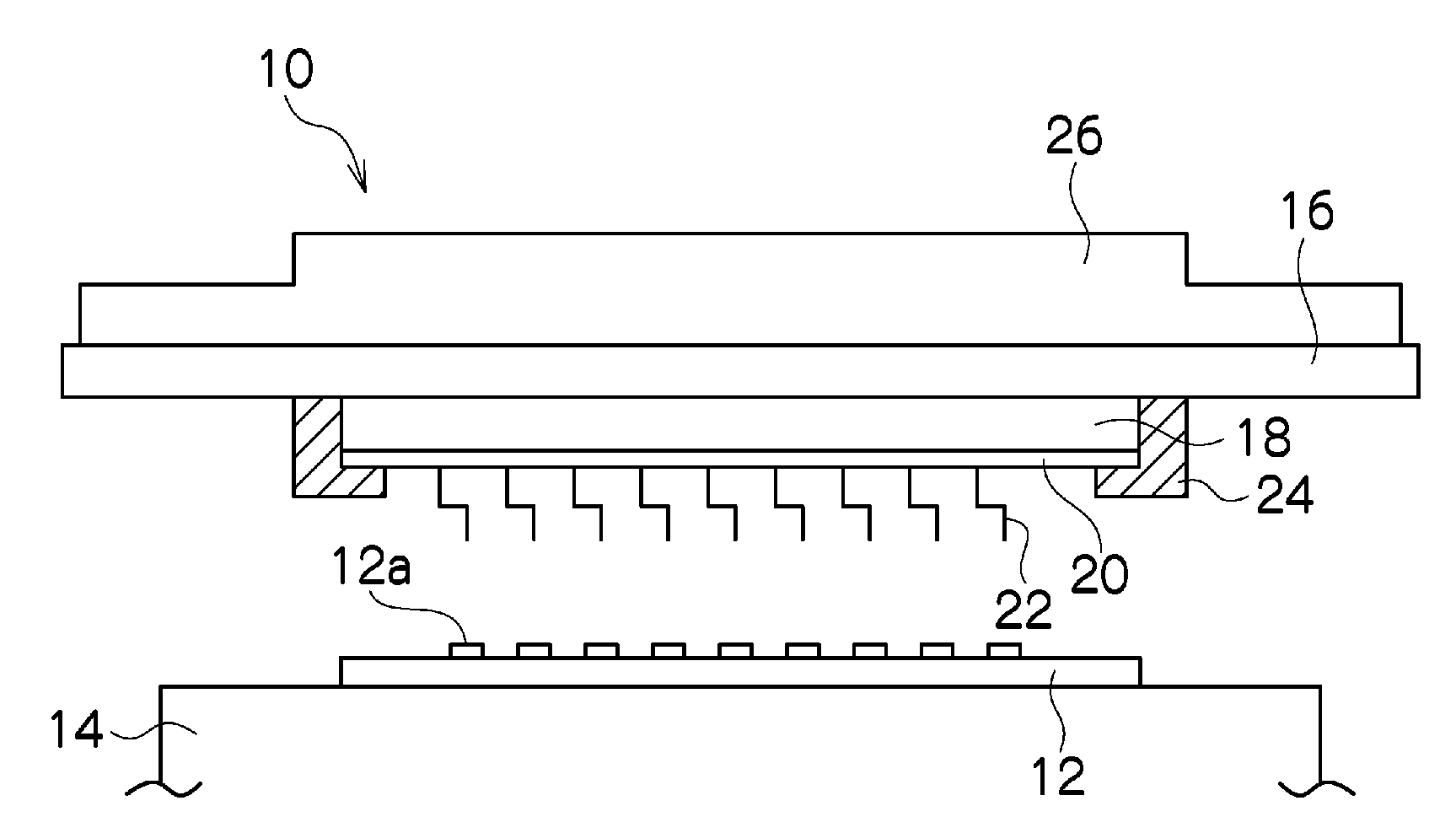
[0043]Hereinafter, a first invention will be described with reference to FIGS. 1 to 6. A probe assembly 10 according to the present invention is used for an electrical test of a plurality of integrated circuits (not shown) formed on a semiconductor wafer 12 as shown in FIG. 1. The semiconductor wafer 12 is removably held on a vacuum chuck 14, for example, with a plurality of electrodes 12a formed on its one surface directing upward. The probe assembly 10 is supported by a frame member (not shown) to be movable relatively to the vacuum chuck 14 in directions approaching and distanced from the semiconductor wafer 12 on the vacuum chuck 14 for the electrical test of the aforementioned integrated circuits of the semiconductor wafer 12 on the vacuum chuck 14.

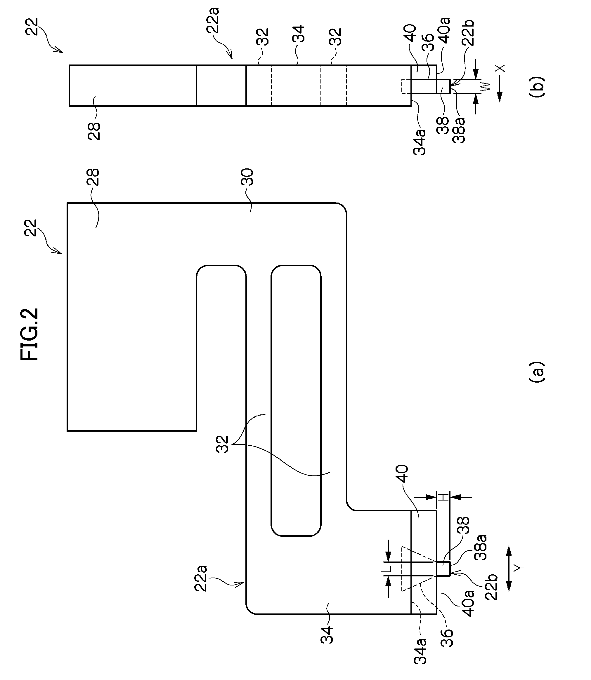
[0044]The probe assembly 10 comprises a printed wiring board 16 and a probe board 20 piled up on the printed wiring board via a ceramic board 18. On one surface of the probe board 20 are arranged and attached a plurality of probes 22...


PUM

PropertyMeasurementUnit
heightaaaaaaaaaa
heightaaaaaaaaaa
thicknessaaaaaaaaaa

Abstract

An electrical test probe comprises a probe tip portion and a probe main body portion having a pedestal portion on which the probe tip portion is formed to be protruded. The probe main body portion is made of a conductive material that is greater in toughness than the probe tip portion, and the probe tip portion is made of a conductive material that is higher in hardness than the material of the probe main body portion. On the pedestal portion is provided a probe tip reinforcement portion that contacts at least one side surface of the probe tip portion, extends toward a tip of the probe tip portion, and permits the tip of the probe tip portion to be protruded from its extending end in the extending direction. Also, the probe tip portion may be in a multi-layer structure having a first metal material layer that is higher in hardness than the tough metal material forming the probe main body portion and a second metal material layer that is greater in toughness than the first metal material layer.

Description

BACKGROUND OF THE INVENTION[0001]The present invention relates to an electrical test probe suitable for use in an electrical test of a plurality of semiconductor integrated circuits formed on a semiconductor wafer and a prove assembly into which this probe is incorporated.[0002]A plurality of semiconductor integrated circuits formed on a semiconductor wafer generally undergo an electrical test before being separated into respective chips to determine whether or not they are manufactured in accordance with the specification. In this electrical test is used a probe assembly comprising electrical test probes to be connected to electrodes of devices under test, that is, the respective semiconductor integrated circuits. The devices under test are connected to a tester via this probe assembly.[0003]One of the conventional probes used for this probe assembly is one comprising a plate-shaped probe main body portion and a probe tip portion provided on the probe main body portion to contact a...

Claims


Application Information

Patent Timeline
Patent Type & Authority Applications(United States)
IPC IPC(8): G01R1/067G01R31/28
CPCG01R1/06733G01R1/06727G01R1/06755G01R1/073H01L22/00
Inventor HIRAKAWA, HIDEKISOMA, AKIRAHAYASHIZAKI, TAKAYUKIKUNIYOSHI, SHINJI
Owner NIHON MICRONICS
Why Eureka
Try Eureka