Multilayer capacitor

a multi-layer capacitor and capacitor technology, applied in the field of multi-layer capacitors, can solve the problems of increasing the difficulty increasing the difficulty of keeping the fluctuations in the power source voltage within tolerances, and increasing the frequency of load current fluctuations, so as to achieve the effect of reducing the equivalent serial inductance, reducing the esl, and increasing the inductan

Active Publication Date: 2008-04-03
TDK CORPARATION
View PDF7 Cites 28 Cited by
  • Summary
  • Abstract
  • Description
  • Claims
  • Application Information

AI Technical Summary

Benefits of technology

[0032] As a result, the action canceling out the magnetic field is occurred at current flow crossing position, so that parasitic inductance of the multilayer capacitor can be smaller, and effect of reducing the equivalent serial inductance is occurred.
[0033] Further, by arranging pluralities of the first internal condu...

Problems solved by technology

Therefore, it has become extremely difficult to keep fluctuations in the power source voltage to within tolerances when faced with rapid changes in the load current.
Along with the increasingly higher operating frequencies of today's CPU's, however, the fluctuations in the load current have become faster and larger.
However, it has been required to further reducing the ESL.
However, in the multi-terminal capacitor, there are problems that preparing a plur...

Method used


Image

  • Multilayer capacitor
  • Multilayer capacitor
  • Multilayer capacitor

Examples


first embodiment

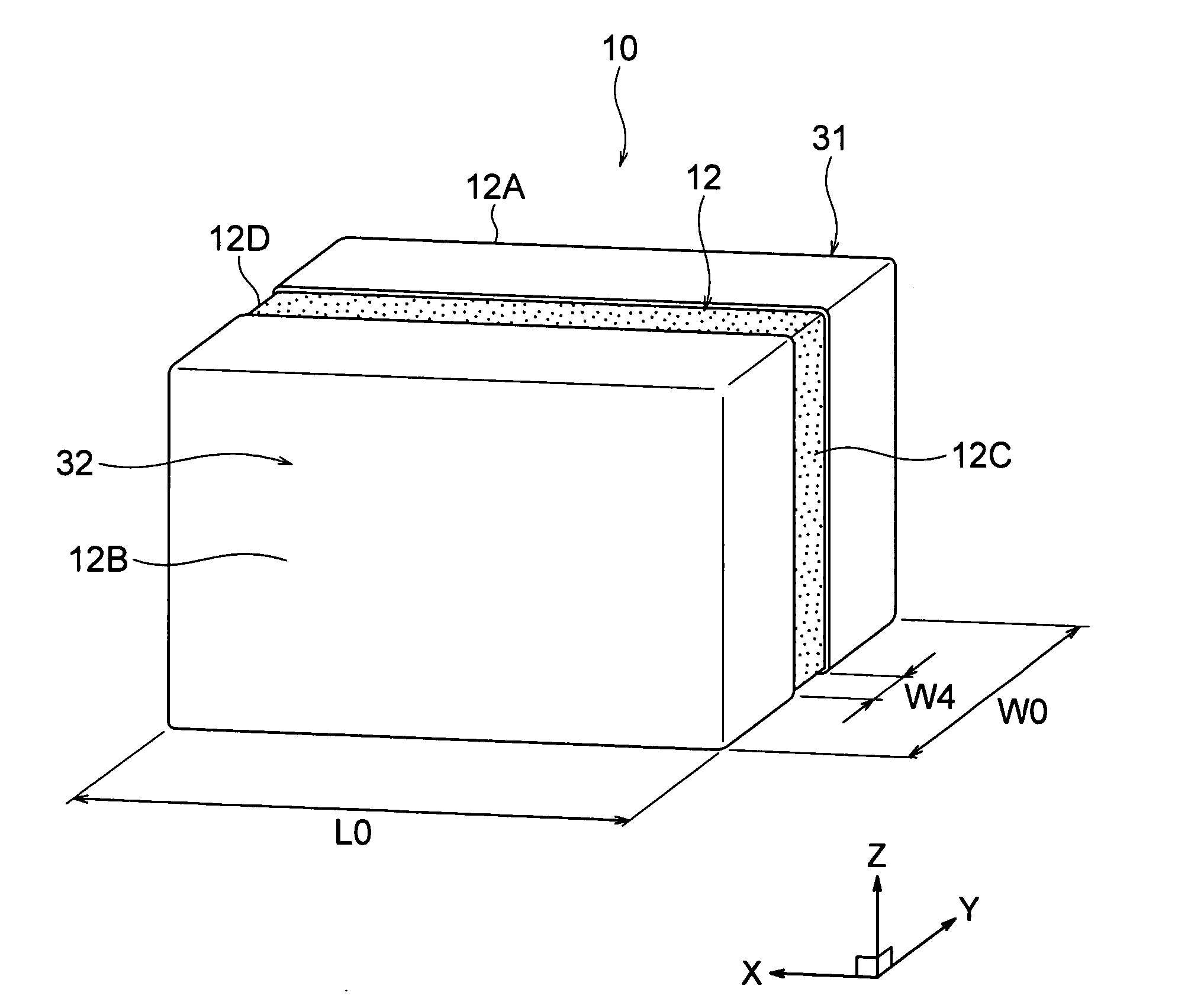
[0048] Whole constitution of a multilayer ceramic capacitor (herein after simply referred to as a “multilayer capacitor”) 10 of a first embodiment of the present invention is specified. As shown in FIG. 1, the multilayer capacitor comprises a dielectric body 12, a rectangular parallelepiped shaped sintered body, obtained by firing a stack of a plurality of ceramic green sheets as dielectric layers.

[0049] The dielectric body 12 comprises a first side face 12A and a second side face 12B opposed to the first side face. Also, the dielectric body 12 comprises a third side face 12C and a fourth side face 14 adjacent to the first side face 12A and the second side face 12B, being parallel to the stacking direction Z of the dielectric layers and opposed each other.

[0050] In the present embodiment, preferably, as shown in FIG. 1, width L0 of the first side face 12A and the second side face 12B in vertical direction to the stacking direction Z (X-direction) of the dielectric layer is larger ...

second embodiment

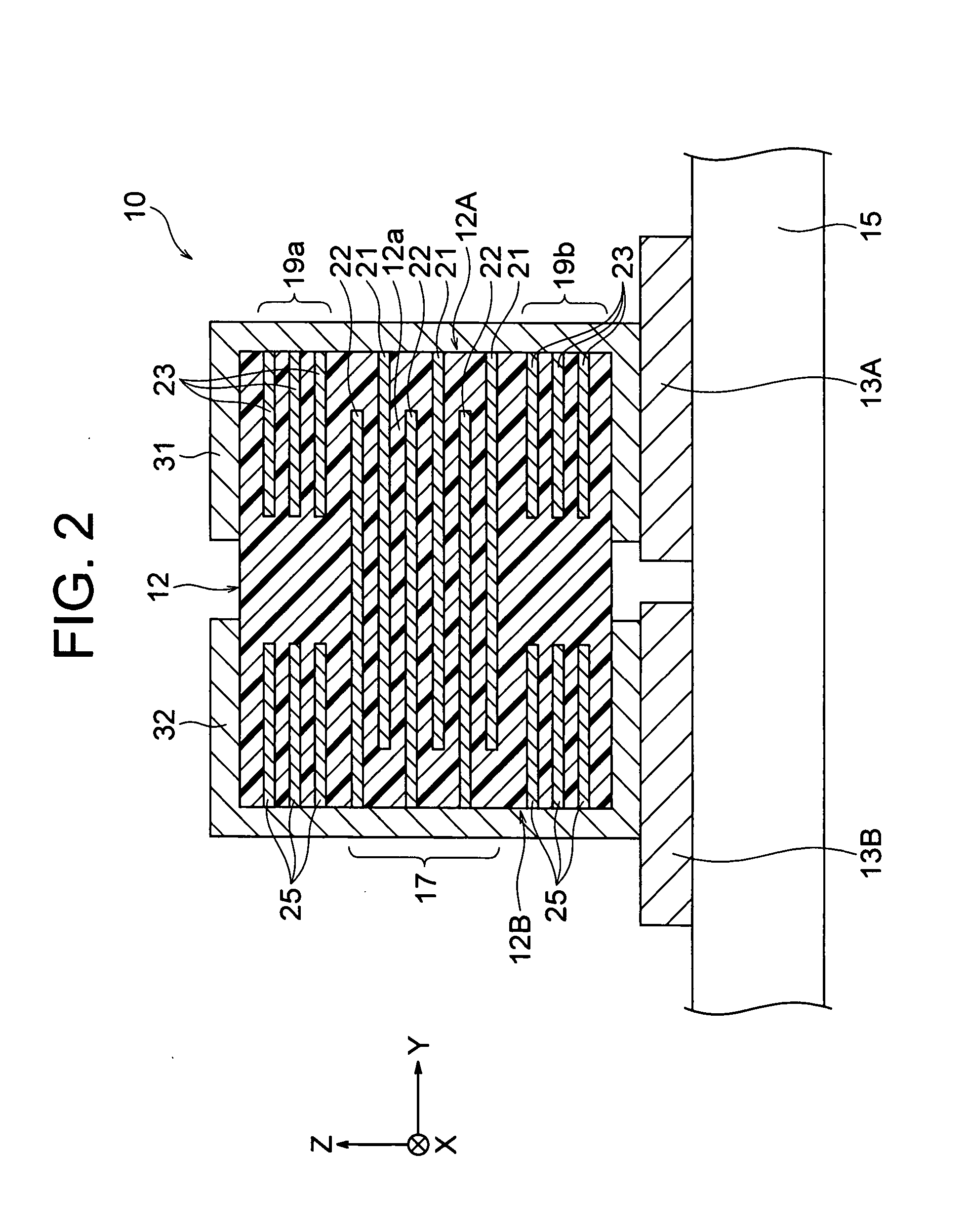
[0083] Next, a second embodiment of the present invention will be explained. Note that, in the following, explanation of common in the first embodiment and the second embodiment are omitted, and only different points of both embodiments will be explained.

[0084] As shown in FIG. 6A, in the present embodiment, in the first lead portion of the first internal conductor layer 21, the first space pattern 41 which is not connected to the first terminal electrode 31 is formed at a center position along with the first longitudinal direction side face 12A. Consequently, the first lead portion comprises a pair of branch lead patterns 21b led out from a main body 21a of the first internal conductor layer 21 to two corner portions wherein the first longitudinal direction side face 12A and the lateral side faces 12C and 12D of the dielectric body 12 are crossing.

[0085] In case that the width of the lateral direction Y of the dielectric body 12 is W0, the width W1 of the lateral direction Y of t...

third embodiment

[0099] Next, a third embodiment of the present invention will be explained based on FIG. 7A to FIG. 7D. Note that, in the following, matters common in the first, the second and the third embodiments are omitted, and only different points of the above embodiments and the third embodiment will be explained.

[0100] In the present embodiment, other than substituting the second internal conductor layer 22 of the second embodiment with two types of the second internal conductor layers 322 shown in FIG. 7B and FIG. 7D and the second internal conductor layers 323 shown in FIG. 7D, a multilayer capacitor is composed in the same way as in the first embodiment.

[0101] In the present embodiment, the second internal conductor layer 322 shown in FIG. 7B is stacked via the dielectric layer 12a under the first internal conductor layer 21 shown in FIG. 7A which is the same as that of the second embodiment, and the first conductor layer 21 shown in FIG. 7C which is the same as the second embodiment i...


PUM


Abstract

A multilayer capacitor 10 of the present invention including: a dielectric body 12 formed by stacking a plurality of dielectric layers 12a; an internal layer portion 17 in which a first and second internal conductor layers 21 and 22 are stacked alternately in the dielectric body 12 via the dielectric layer 12a; external layer portions 19a and 19b in which a first and second external conductor layers 23 and 25 are stacked via the dielectric layer 12a; a first terminal electrode 31 connected with the first internal conductor layer 21 and the first external conductor layer 23, formed at least on a first side face 12A of the dielectric body 12; and a second terminal electrode 32 connected with the second internal conductor layer 22 and the second external conductor layer 25, formed at least on a second side face 12B opposed to the first side face 12A.

Description

BACKGROUND OF THE INVENTION [0001] 1. Field of the Invention [0002] The present invention relates to multilayer capacitor greatly reducing the equivalent serial inductance (ESL), more particularly relates to a multilayer capacitor used as a decoupling capacitor. [0003] 2. Description of the Related Art [0004] In recent years, while advances have been made in reducing the voltage of power sources used for supplying power to large-scale integrated circuits (LSI's) and other integrated circuits, the load current has increased. [0005] Therefore, it has become extremely difficult to keep fluctuations in the power source voltage to within tolerances when faced with rapid changes in the load current. Therefore, a decoupling capacitor (for example two-terminal structure multilayer ceramic capacitor) is now being connected to a power source. At the time of transitory fluctuation in the load current, current is supplied from this multilayer ceramic capacitor to the LSI of the central processi...

Claims


Application Information

Patent Timeline
IPC IPC(8): H01G4/005
CPCH01G4/012H01G4/30H01G4/232Y02E60/10H01M4/30
Inventor TOGASHI, MASAAKI
Owner TDK CORPARATION
Why Eureka
Try Eureka