Process for forming a film, piezoelectric film, piezoelectric device, and liquid discharge apparatus

Active Publication Date: 2008-04-03
FUJIFILM CORP
View PDF4 Cites 13 Cited by
  • Summary
  • Abstract
  • Description
  • Claims
  • Application Information

AI Technical Summary

Benefits of technology

[0011]The primary object of the present invention is to clarify factors of film formation conditions, which factors have effects upon film characteristics in a vapor phase growth technique utilizing plasma, such as a sputterin

Problems solved by technology

As for piezoelectric films, which contain Pb-containing perovskite type oxides, such as PZT, the problems are encountered in that, in cases where the film formation is performed at high temperatures, a Pb-poor state is apt to occur.
Regardless of whether Pb is or is not contained, in cases where the film formation temperature is

Method used


Image

  • Process for forming a film, piezoelectric film, piezoelectric device, and liquid discharge apparatus
  • Process for forming a film, piezoelectric film, piezoelectric device, and liquid discharge apparatus
  • Process for forming a film, piezoelectric film, piezoelectric device, and liquid discharge apparatus

Examples


example 1

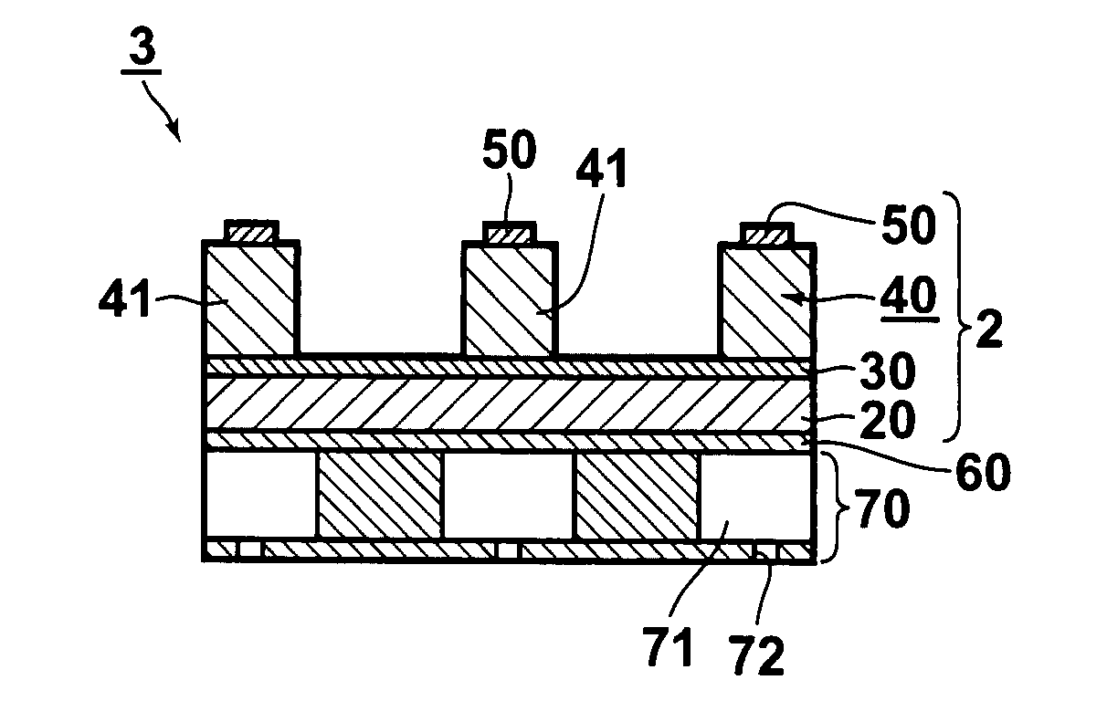
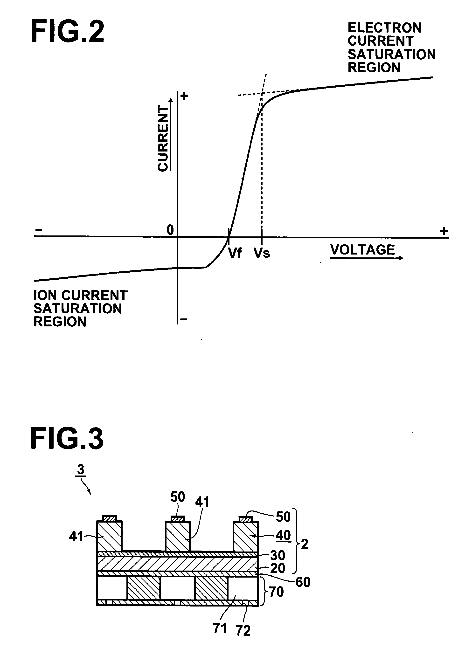
[0145]A piezoelectric film containing PZT or Nb-doped PZT was formed by use of the sputtering apparatus as illustrated in FIG. 1, under the conditions of a vacuum degree of 0.5 Pa and in an Ar / O2 mixed atmosphere (O2 volume fraction: 2.5%), by use of a target of Pb1.3Zr0.52Ti0.48O3 or Pb1.3Zr0.43Ti0.44Nb0.13O3. The Nb-doped PZT will hereinbelow be referred to as Nb-PZT.

[0146]As a base plate for film formation, an electrode-fitted base plate, in which a 30 μm-thick Ti close contact layer and a 150 nm-thick Pt bottom electrode had been overlaid in this order on an Si wafer, was prepared. The base plate / target distance was set at 60 mm.

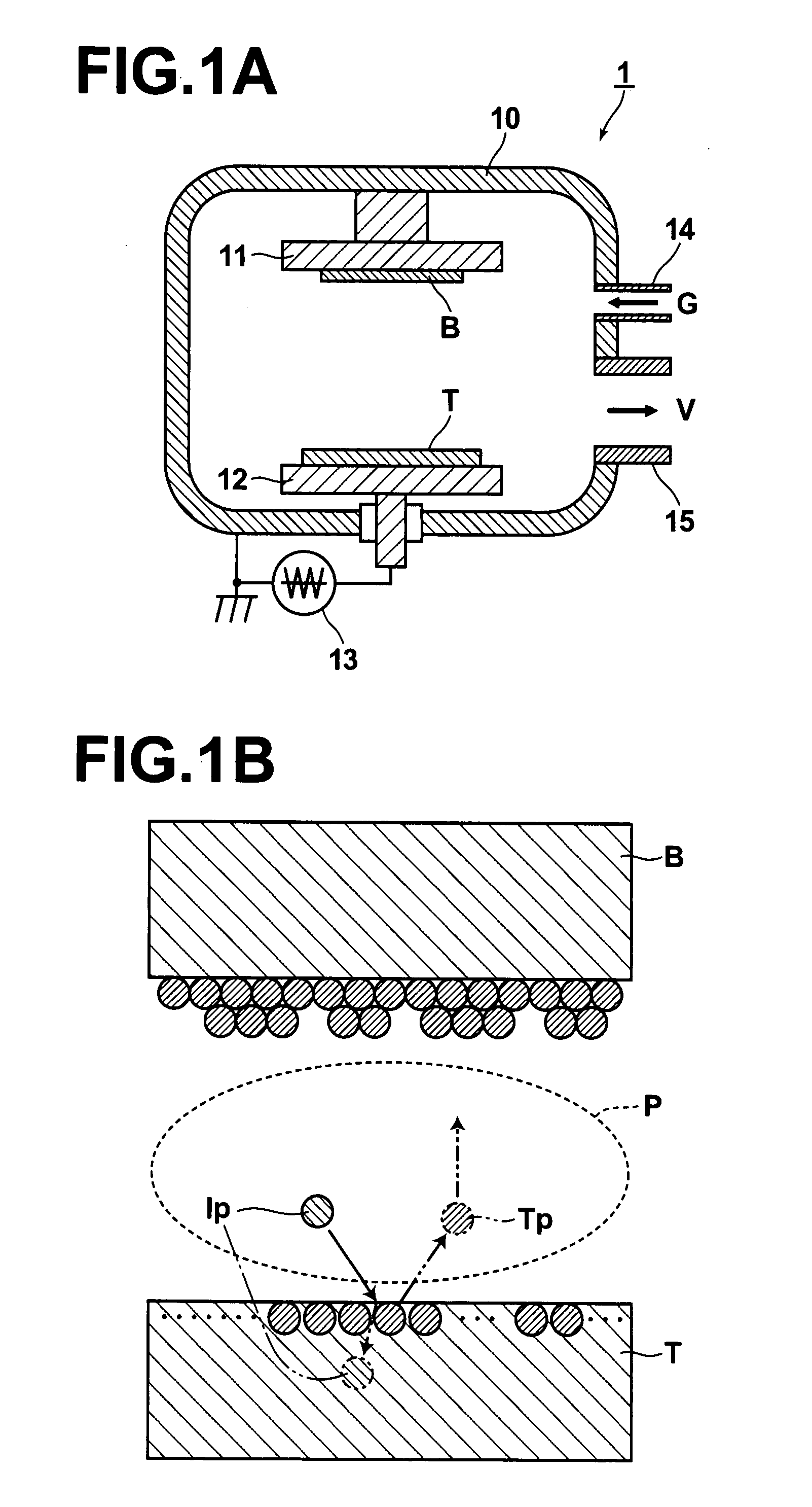
[0147]The base plate was set in the floating state, a ground wire was located at a position, which was spaced apart from the base plate and which was outside of a region between the target and the base plate, and the film formation was performed. At this time, the plasma potential Vs and the floating potential (the potential in the vicinity of the base p...

example 2

[0154]A ground wire was located in the vicinity of the base plate in order for the plasma state of the apparatus to be altered, and the film formation was thus performed. At this time, as in Example 1, the plasma potential Vs and the floating potential Vf were measured. It was found that Vs−Vf=approximately 42V. Under the plasma conditions described above, the PZT film formation was performed with the film formation temperature Ts being set at various difference values within the range of 380° C. to 500° C. As for the obtained films, the XRD measurement was performed. FIG. 8 illustrates the XRD patterns of the principal films.

[0155]As illustrated in FIG. 8, under the conditions of the difference Vs−Vf (V)=approximately 42, the perovskite crystal having good crystal orientational characteristics was obtained at the film formation temperature Ts=420° C. Therefore, the film formation temperature Ts 420° C. was judged as being “”. At the film formation temperature Ts of at most 400° C....

example 3

[0157]The difference Vs−Vf (V) was altered through alteration of the position of the ground wire, and the film formation of the PZT film or the Nb-PZT film were performed. Also, the evaluation was made in the same manner as that in Example 2. With respect to each of the conditions of the difference Vs−Vf (V)=approximately 22, approximately 32, approximately 45, and approximately 50, the film formation temperature Ts was set at various different values, and the film formation was performed. In Examples 1, 2, and 3, the samples having been formed under the film formation conditions of the film formation temperature Ts=525° C. and the difference Vs−Vf (V)=approximately 12, approximately 32, and approximately 45 were the Nb-PZT films. The other samples were the PZT films.

[0158]FIG. 10 shows an example of the sample, which was associated with the XRD measurement results judged as being “×”. FIG. 10 illustrates the XRD pattern of the Nb-PZT film, which was formed under the conditions of t...


PUM

PropertyMeasurementUnit
Dielectric polarization enthalpyaaaaaaaaaa
Metallic bondaaaaaaaaaa
Piezoelectricityaaaaaaaaaa

Abstract

Film formation conditions are determined in accordance with relationships among a film formation temperature Ts (° C.), a difference Vs−Vf (V), which is the difference between a plasma potential Vs (V) in the plasma at the time of the film formation and a floating potential Vf (V), and characteristics of the formed film. For a piezoelectric film containing at least one kind of Pb-containing perovskite type oxide, the film formation conditions should preferably be determined within a range such that Formulas (1) and (2) shown below are satisfied:
Ts(° C.)≧400   (1)
−0.2Ts+100<Vs−Vf(V)<−0.2Ts+130   (2)

Description

BACKGROUND OF THE INVENTION[0001]1. Field of the Invention[0002]This invention relates to a process for forming a film, in which the film is formed with a vapor phase growth technique utilizing plasma, and a piezoelectric film having been formed by use of the process for forming a film. This invention also relates to a piezoelectric device, which comprises the piezoelectric film, and a liquid discharge apparatus, which is provided with the piezoelectric device.[0003]2. Description of the Related Art[0004]Piezoelectric devices provided with a piezoelectric film, which has piezoelectric characteristics such that the piezoelectric film expands and contracts in accordance with an increase and a decrease in electric field applied across the piezoelectric film, and electrodes for applying the electric field across the piezoelectric film have heretofore been used as actuators to be loaded on ink jet type recording heads, and the like. As piezoelectric materials, there have heretofore been ...

Claims


Application Information

Patent Timeline
IPC IPC(8): H01L41/00C23C16/00B41J2/14B41J2/16C23C14/08C23C14/34C23C16/50H01L21/316H01L41/09H01L41/18H01L41/316H01L41/39
CPCB41J2/161B41J2/1646C23C14/08C23C14/088H01L41/316C23C14/548H01L41/0805H01L41/1876C23C14/345H10N30/1051H10N30/8554H10N30/076
Inventor FUJII, TAKAMICHISAKASHITA, YUKIO
Owner FUJIFILM CORP
Why Eureka
Try Eureka