Methods for uniform doping of non-planar transistor structures

Inactive Publication Date: 2008-04-10
INTEL CORP
View PDF2 Cites 80 Cited by
  • Summary
  • Abstract
  • Description
  • Claims
  • Application Information

AI Technical Summary

Problems solved by technology

This is due to the proximity of the top and side gates relative to one another which causes full depletion and results in steeper sub-threshold gradients (SG) and smaller drain induced barrier lowe

Method used


Image

  • Methods for uniform doping of non-planar transistor structures
  • Methods for uniform doping of non-planar transistor structures
  • Methods for uniform doping of non-planar transistor structures

Examples


Embodiment Construction

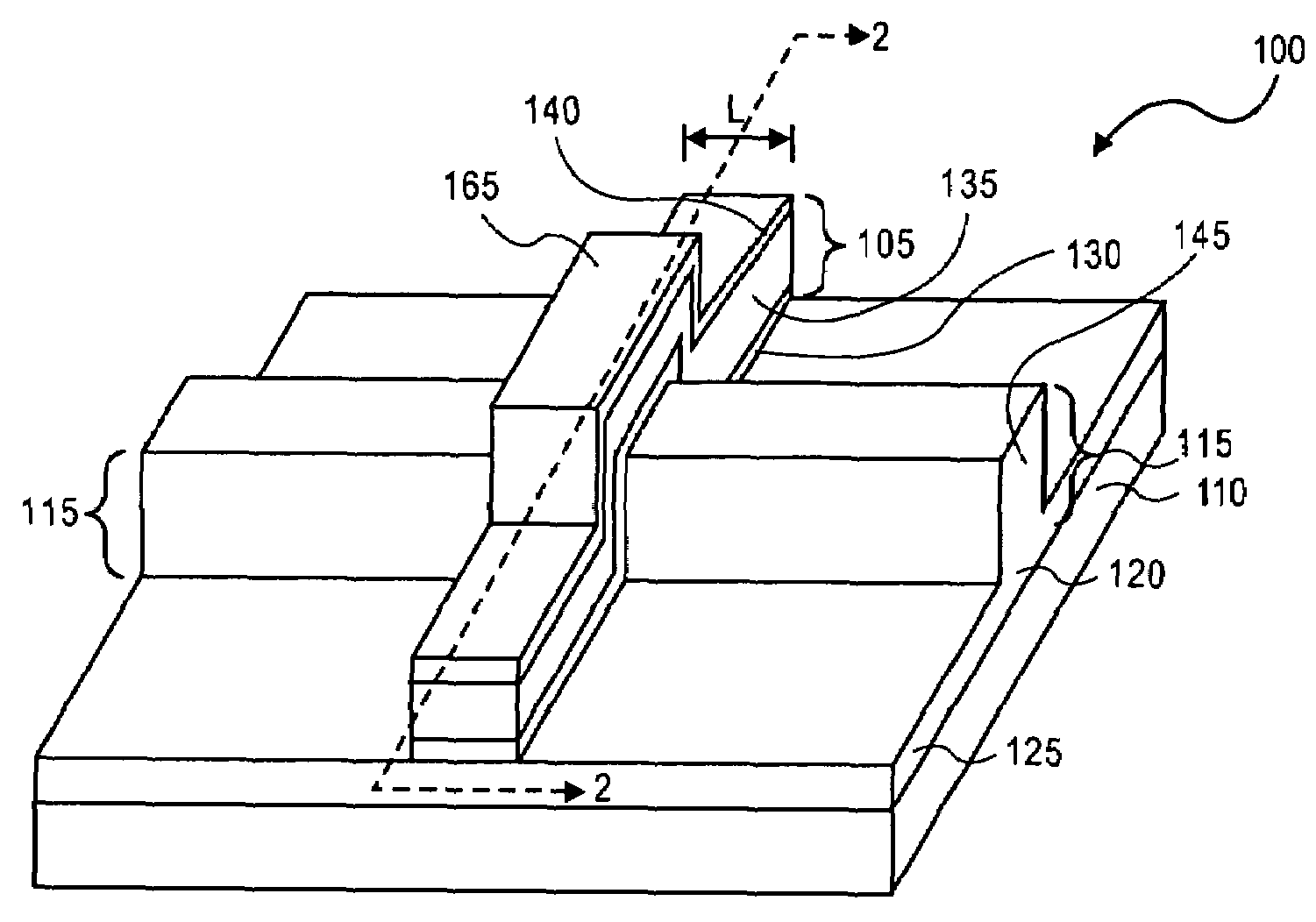
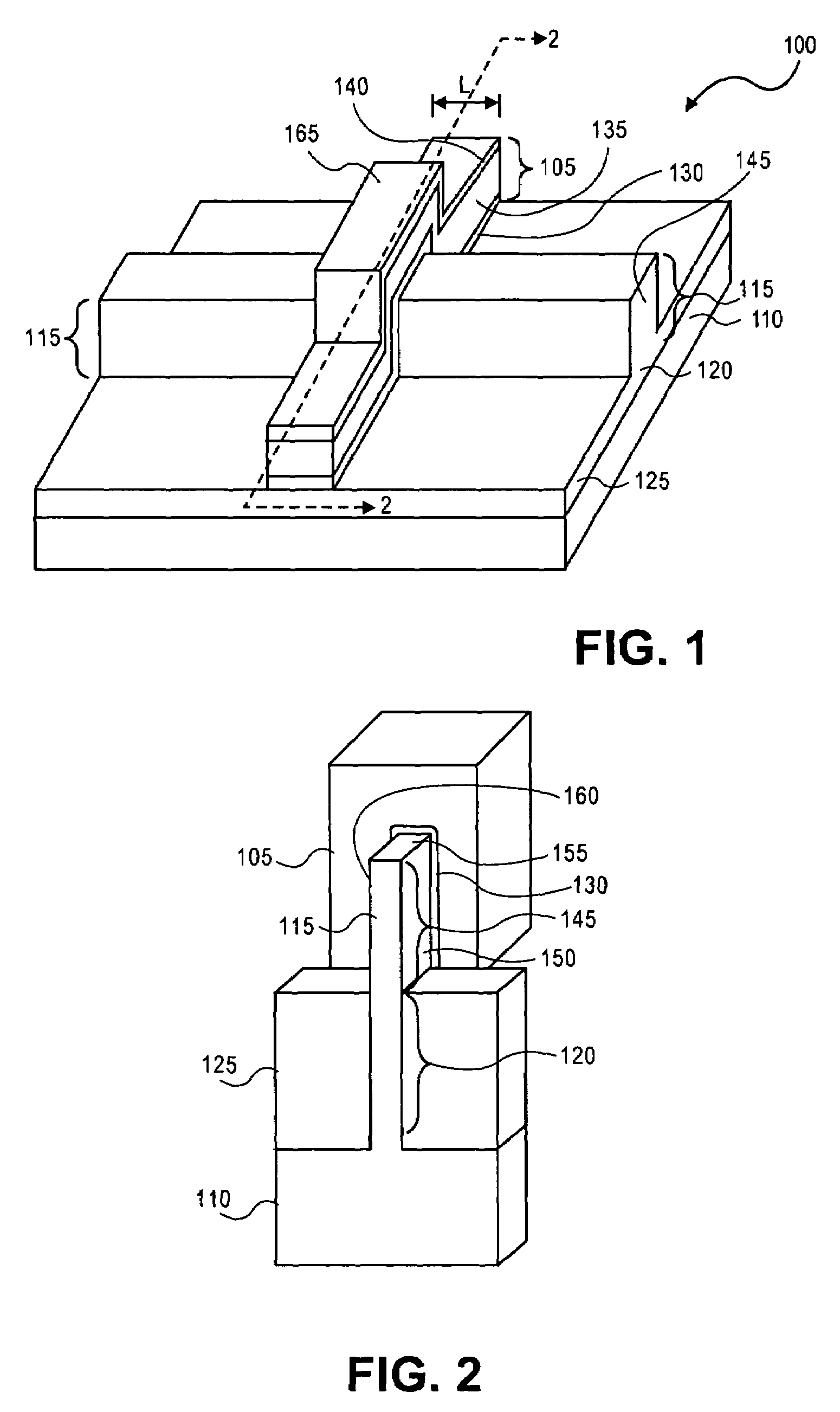
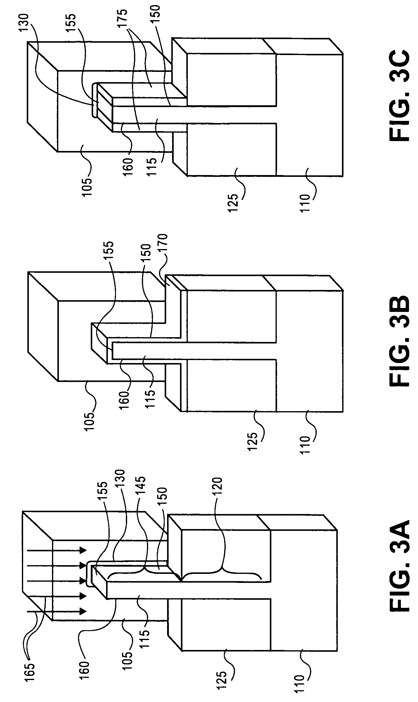
[0015]FIG. 1 illustrates a perspective view of an embodiment of a tri-gate structure which forms a portion of a circuit substrate. Structure 100 can include gate structure 105 formed on substrate 110 and on a portion of silicon body 115, i.e., silicon fin. “Silicon body” and “silicon fin” are hereinafter referred to interchangeably. Substrate 110 can be bulk silicon or silicon-on-insulator (SOI). Silicon fin 115 is in a different plane relative to substrate 110 and is situated perpendicular relative to gate structure 105. In some applications, structure 100 is referred to as a non-planar transistor.

[0016]In one embodiment, substrate 110 can be composed of a single crystal semiconductor material, which can be, for example, silicon or germanium. Silicon fin 115 can be composed of a semiconductor material such as silicon. Silicon fin 115 includes buried section 120, which lies below the surface of the plane of structure 100 and buried within oxide layer 125, and non-planar section 145....


PUM


Abstract

Methods for uniformly tip doping a silicon body of a non-planar transistor and devices and systems formed by such methods. In one embodiment, a method can include vertical tip ion implantation of a silicon body with at least three surfaces on a substrate followed by conformal deposition of a dielectric material. The dielectric material can be selectively etched to expose a top surface of the silicon body followed by selective re-oxidation of the top surface for form a mask. The remaining dielectric material can be removed followed by angled ion implantation of at least two sidewalls of the silicon body. The mask can be removed resulting in a silicon body with uniform doping.

Description

FIELD OF INVENTION[0001]Integrated circuit structures.BACKGROUND OF INVENTION[0002]A recent development in semiconductor processing is the tri-gate transistor, or non-planar transistor. A tri-gate transistor includes a thin semiconductor body (e.g., a silicon fin) formed on a substrate and having a top surface and two sidewall surfaces perpendicular to the top surface. A gate structure is formed on the substrate and the silicon fin perpendicular to the silicon fin. Source and drain regions are formed in the fin on opposite sides of the gate structure. Because the gate structure surrounds the silicon fin on the three surfaces, the transistor essentially has three separate gates. These three separate gates provide three separate channels for electrical signals to travel, thus effectively tripling the conductivity as compared to a conventional planar transistor.[0003]Tri-gate transistors generally have superior performance to bulk gate devices. This is due to the proximity of the top a...

Claims


Application Information

Patent Timeline
IPC IPC(8): H01L21/8238H01L29/94
CPCH01L21/2236H01L21/26586H01L29/7851H01L29/66803H01L21/823437
Inventor DOYLE, BRIANCHAU, ROBERTDATTA, SUMANKAVALIEROS, JACK
Owner INTEL CORP
Why Eureka
Try Eureka