Eureka AIR delivers breakthrough ideas for toughest innovation challenges, trusted by R&D personnel around the world.

Method for manufacturing semiconductor device layer

A semiconductor and device layer technology, applied in the fields of semiconductor devices, semiconductor/solid-state device manufacturing, electrical components, etc., can solve problems such as lattice voids, oxygen-enhanced diffusion, and high concentration of short-channel dopants, and achieve improved performance. Effect

Inactive Publication Date: 2011-06-15
SEMICON MFG INT (SHANGHAI) CORP
View PDF1 Cites 8 Cited by
  • Summary
  • Abstract
  • Description
  • Claims
  • Application Information

AI Technical Summary

Problems solved by technology

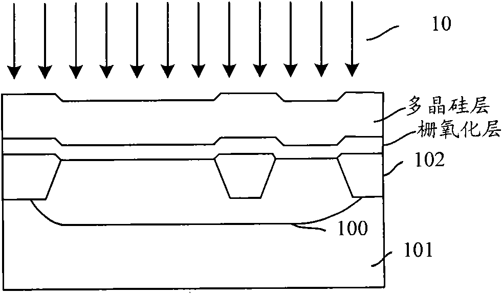
[0026] When the re-oxidation step is carried out in the fourth step of the above process, since the chemical vapor deposition method is used, the reaction chamber is heated at a low temperature during the process, which will cause the oxygen-enhanced diffusion of the dopant in the first step when the well 100 is manufactured. (OED) phenomenon, lattice damage will occur near the surface area of ​​the substrate 101 of the semiconductor device, and lattice voids will appear
In this way, in the process of lightly doping to form a shallow junction in Step 5, a Transient Enhanced Diffusion (TED) phenomenon will appear in the substrate 101 of the semiconductor device near the surface region, resulting in a large dopant concentration in the short channel, which is harmful to the The short channel of semiconductor devices produces short channel damage (SCE) and reverse short channel damage (RSCE), which reduces the performance of the final semiconductor device

Method used


Image

  • Method for manufacturing semiconductor device layer
  • Method for manufacturing semiconductor device layer
  • Method for manufacturing semiconductor device layer

Examples


Embodiment Construction

[0042] In order to make the object, technical solution and advantages of the present invention clearer, the present invention will be further described in detail below with reference to the accompanying drawings and examples.

[0043]In the prior art, the TED phenomenon during light doping to form a shallow junction is the main cause of SCE and RSCE in the short channel of the semiconductor device, thereby reducing the performance of the final manufactured semiconductor device. To solve this problem, there are three ways. Among them, one way is: reducing the energy of ion implantation or / and reducing the concentration of shallow doping impurities. However, this is at the expense of reducing the performance of the final semiconductor device, and is generally not used; the second method is: during ion implantation in the process of light doping to form a shallow junction, lightly doped impurities and carbon are ion implanted together , so that carbon can fill the gaps between t...


PUM


Abstract

The invention discloses a method for manufacturing a semiconductor device layer. The method comprises the following steps of: after a well is formed on a substrate of a semiconductor device, forming an isolation shallow trench, and forming a grid on the substrate of the semiconductor device; performing ion implantation of carbon impurity on the grid and the substrate of the semiconductor device; after the surface of the grid and the surface of the substrate of the semiconductor device are re-oxidized, performing light dope on the grid and the substrate of the semiconductor device to form a shallow junction on the substrate of the semiconductor device; forming a nitrogen oxide side wall of the grid, doping the grid and the substrate of the semiconductor device, and performing deposition on the semiconductor device to form a drain and a source; and depositing metals on the surface of the grid and the semiconductor substrate by adopting a self-alignment silicide method to form metalized silicon layers, then performing quick annealing treatment, and etching the un-reacted metals. The method can effectively reduce the transient enhanced diffusion (TED) generated in the re-oxidation process of the grid so as to remarkably prevent the short trench of the semiconductor device from generating short channel effect (SCE) and reverse short channel effect (RSCE).

Description

technical field [0001] The invention relates to semiconductor manufacturing technology, in particular to a method for manufacturing semiconductor device layers. Background technique [0002] With the wide application of electronic equipment, the manufacturing process of semiconductors has been developed rapidly, the feature size of semiconductor devices is getting smaller and smaller, and the manufacturing of device layers in semiconductor devices is becoming more and more important. The device layer of the semiconductor device here refers to the manufacturing of the source, drain and gate on the semiconductor substrate. Among them, the shallow junction fabrication in the device layer of the semiconductor device becomes a key factor affecting the performance of the device layer of the final semiconductor device. [0003] Figure 1a-1f Shown is a cross-sectional structural view of device layer fabrication of a prior art semiconductor device. The device layer manufacturing p...

Claims


Application Information

Patent Timeline
IPC IPC(8): H01L21/8238H01L21/28
Inventor 赵猛
Owner SEMICON MFG INT (SHANGHAI) CORP
Why Eureka
Eureka Blog
Learn More