

Method for modulating stresses of a contact etch stop layer
a technology of contact etching and stress, which is applied in the direction of semiconductor devices, basic electric elements, electrical equipment, etc., can solve the problems of high cost of introducing different stresses, high dielectric constant of cesl films, and constant effort in scaling of vlsi circuits
- Summary
- Abstract
- Description
- Claims
- Application Information
AI Technical Summary
Benefits of technology
Problems solved by technology
Method used
Image

Examples
Embodiment Construction
[0016]The making and using of the presently preferred embodiments are discussed in detail below. It should be appreciated, however, that the present invention provides many applicable inventive concepts that can be embodied in a wide variety of specific contexts. The specific embodiments discussed are merely illustrative of specific ways to make and use the invention, and do not limit the scope of the invention.
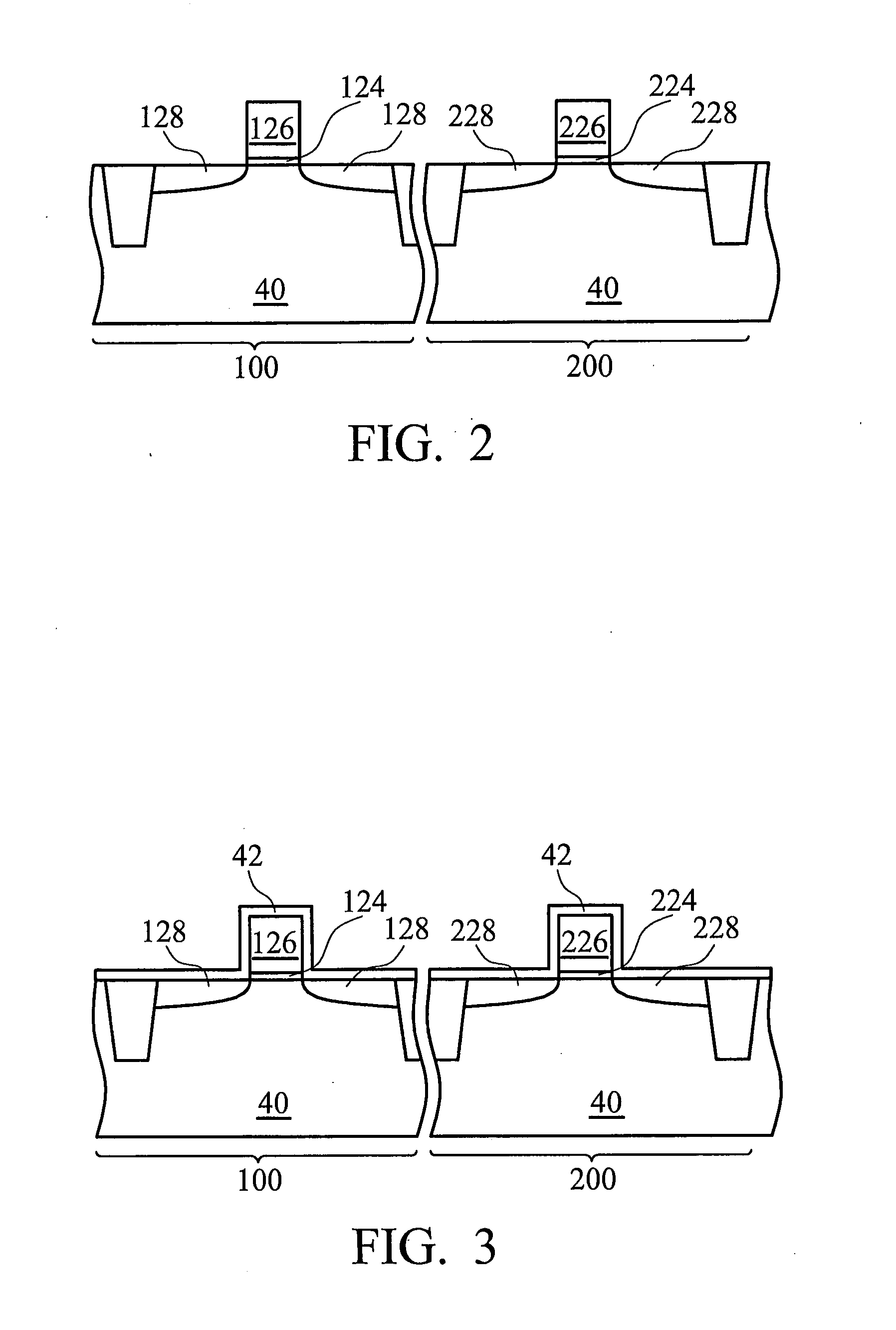
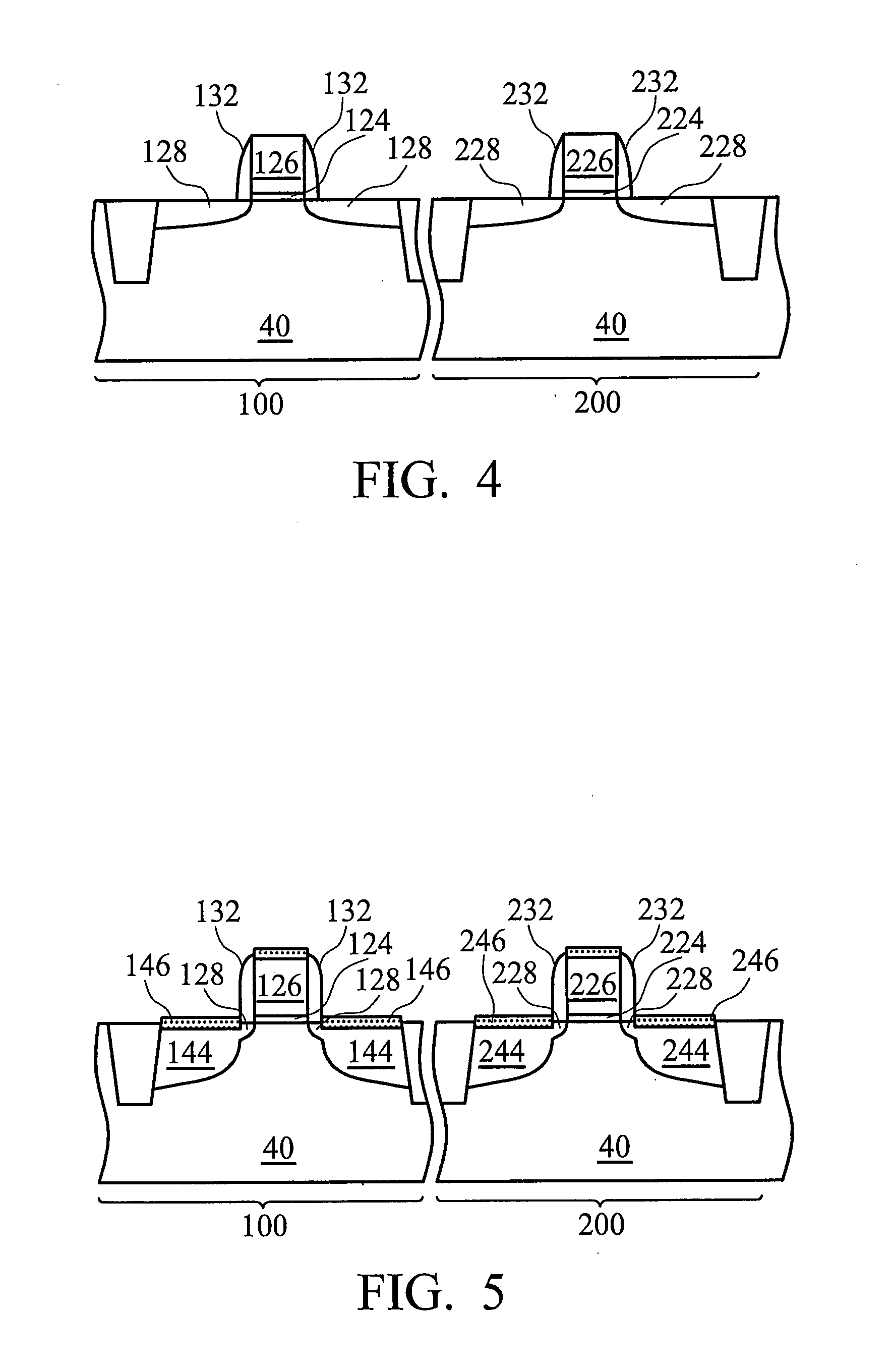
[0017]A method for modulating stresses after the formation of a stressed layer is illustrated in FIGS. 2 through 7. Throughout the various views and illustrative embodiments of the present invention, like reference numbers are used to designate like elements.
[0018]Referring to FIG. 2, a substrate 40 is provided. Substrate 40 can be formed of common substrate materials such as silicon, SiGe, stressed silicon on SiGe, silicon on insulator (SOI), silicon germanium on insulator (SGOI), germanium on insulator (GOI), and the like. Substrate 40 preferably includes device regions 100...
PUM
 Abstract
Description
Claims
Application Information