

Ald of metal silicate films
a metal silicate film and siosub>2 technology, applied in the field of metal silicate films, can solve the problems of unreliable thin film, adversely affecting device performance, and difficult to obtain traditional methods full film coverage on deep bottoms and vias
Active Publication Date: 2008-04-10
ASM IP HLDG BV
View PDF99 Cites 268 Cited by
- Summary
- Abstract
- Description
- Claims
- Application Information
AI Technical Summary
Problems solved by technology
Design rules are setting the feature sizes to ≦0.2 μm, making complete film coverage on deep bottoms and vias difficult to obtain using traditional methods.
Additionally, with decreasing feature sizes, quantum mechanical tunneling (“tunneling”) leads to leakage current, i.e., current leaking out of device features (e.g., across gate oxides), which adversely affects device performance.
For this reason, substantially thin SiO2 films are unreliable as gate dielectrics (gate oxides), for example, in MOSFET (metal-oxide-semiconductor field-effect transistor) devices.
However, with decreasing features sizes, it has become increasingly difficult to deposit hafnium silicate films with compositional and thickness uniformities suited for current and future generation of ICs.
However, a limitation of the conventional processes described above is that the maximum silicon content achievable is about 65%, rendering the method unsuitable for applications in which metal silicate films with a silicon content greater than 65% are desired.
Method used
View moreImage
Smart ImageViewing Examples

Examples
example 1
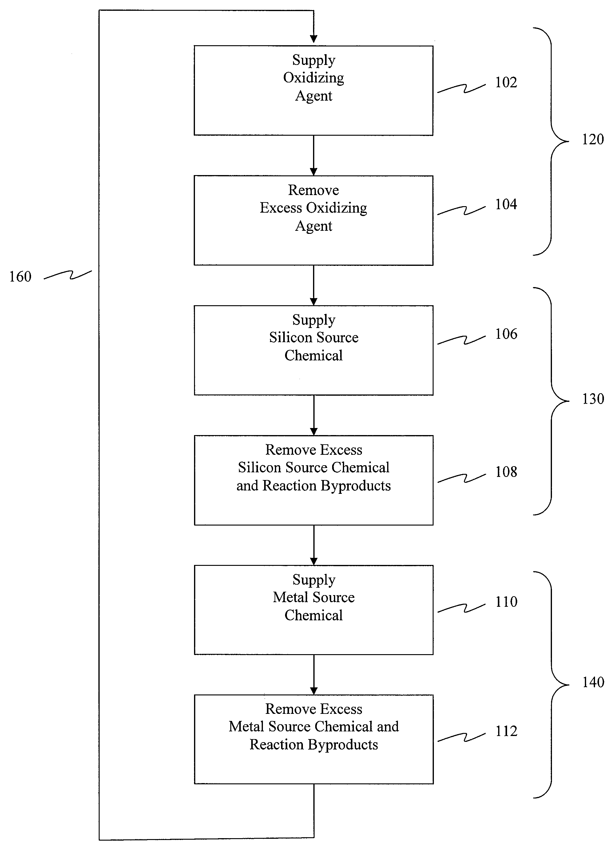
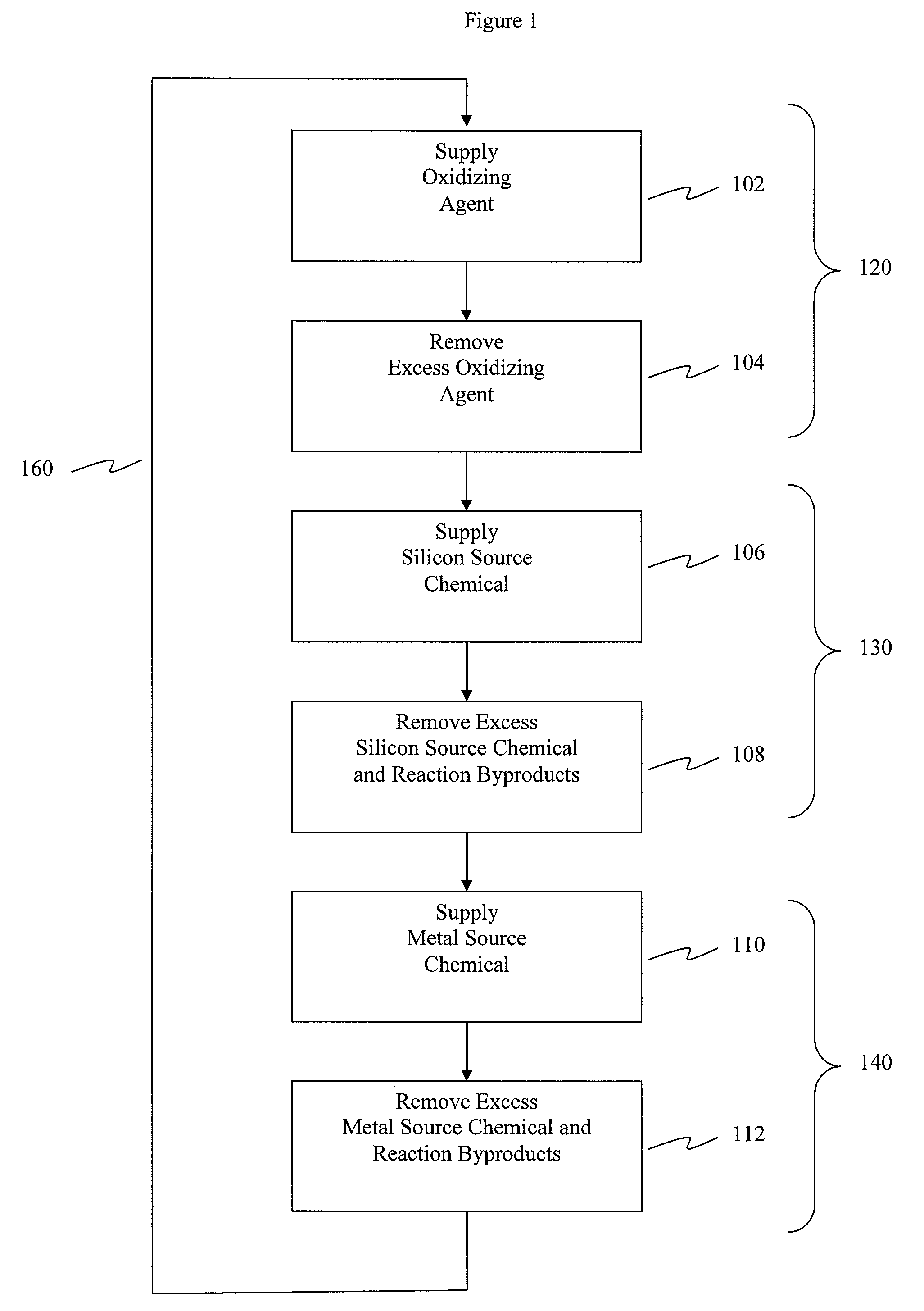
[0070]A hafnium silicate film was deposited on a 300 mm silicon wafer using a Pulsar™ reactor manufactured by ASM America, Inc. Deposition was conducted at a substrate temperature in the range of about 300 to 350° C. The sequence processing steps included the following:
[0071](1) H2O pulse;
[0072](2) N2 purge;
[0073](3) SiCl4 pulse;
[0074](4) N2 purge;
[0075](5) HfCl4 pulse; and
[0076](6) N2 purge.
[0077]Steps (1)-(6) were repeated until a hafnium silicate film with a thickness of about 40 Å was formed on the silicon wafer.
[0078]In at least some of the aforesaid embodiments, any element used in an embodiment can interchangeably be used in another embodiment unless such a replacement is not feasible.
Login to View More PUM
| Property | Measurement | Unit |
|---|---|---|
| Temperature | aaaaa | aaaaa |
| Temperature | aaaaa | aaaaa |
| Temperature | aaaaa | aaaaa |
Abstract
Methods for forming metal silicate films are provided. The methods comprise contacting a substrate with alternating and sequential vapor phase pulses of a silicon source chemical, metal source chemical, and an oxidizing agent, wherein the metal source chemical is the next reactant provided after the silicon source chemical. Methods according to some embodiments can be used to form silicon-rich hafnium silicate and zirconium silicate films with substantially uniform film coverages on substrate surface.
Description
REFERENCE TO RELATED APPLICATIONS[0001]This application claims the benefit of U.S. Provisional Patent Application No. 60 / 850,082, filed Oct. 5, 2006. The present application is related to U.S. patent application Ser. No. 10 / 148,525 to Tois et al., filed May 31, 2002, U.S. patent application Ser. No. 10 / 678,766 to Tois et al., filed Oct. 3, 2003, and U.S. patent application Ser. No. 11 / 490,875 to Wang et al., filed Jul. 21, 2006. The entirety of each of the above-referenced applications is incorporated herein by reference and made part of this specification.BACKGROUND[0002]1. Field of the Disclosure[0003]The present disclosure relates to metal silicate films. In particular, the disclosure concerns methods for forming silicon-rich metal silicate films by atomic layer deposition (ALD) and the films formed by such methods.[0004]2. Description of the Related Art[0005]The integration level of components in integrated circuits is increasing, which rapidly places a demand for a decrease of ...
Claims
Login to View More Application Information
Patent Timeline
 IPC IPC(8): H01L21/31C01B33/20
CPCC23C16/401C23C16/45531C23C16/405H01L21/0262H01L21/0228
InventorWANG, CHANG-GONGSHERO, ERICWILK, GLEN
OwnerASM IP HLDG BV