
Semiconductor device and method of fabricating the same

a semiconductor and semiconductor technology, applied in the direction of semiconductor devices, basic electric elements, electrical equipment, etc., can solve the problems of increasing the difficulty of filling the element isolation region sufficiently, increasing the etching rate, etc., to prevent cracking and suppress peeling

Inactive Publication Date: 2008-04-17
KK TOSHIBA
View PDF16 Cites 19 Cited by
  • Summary
  • Abstract
  • Description
  • Claims
  • Application Information

AI Technical Summary

Benefits of technology

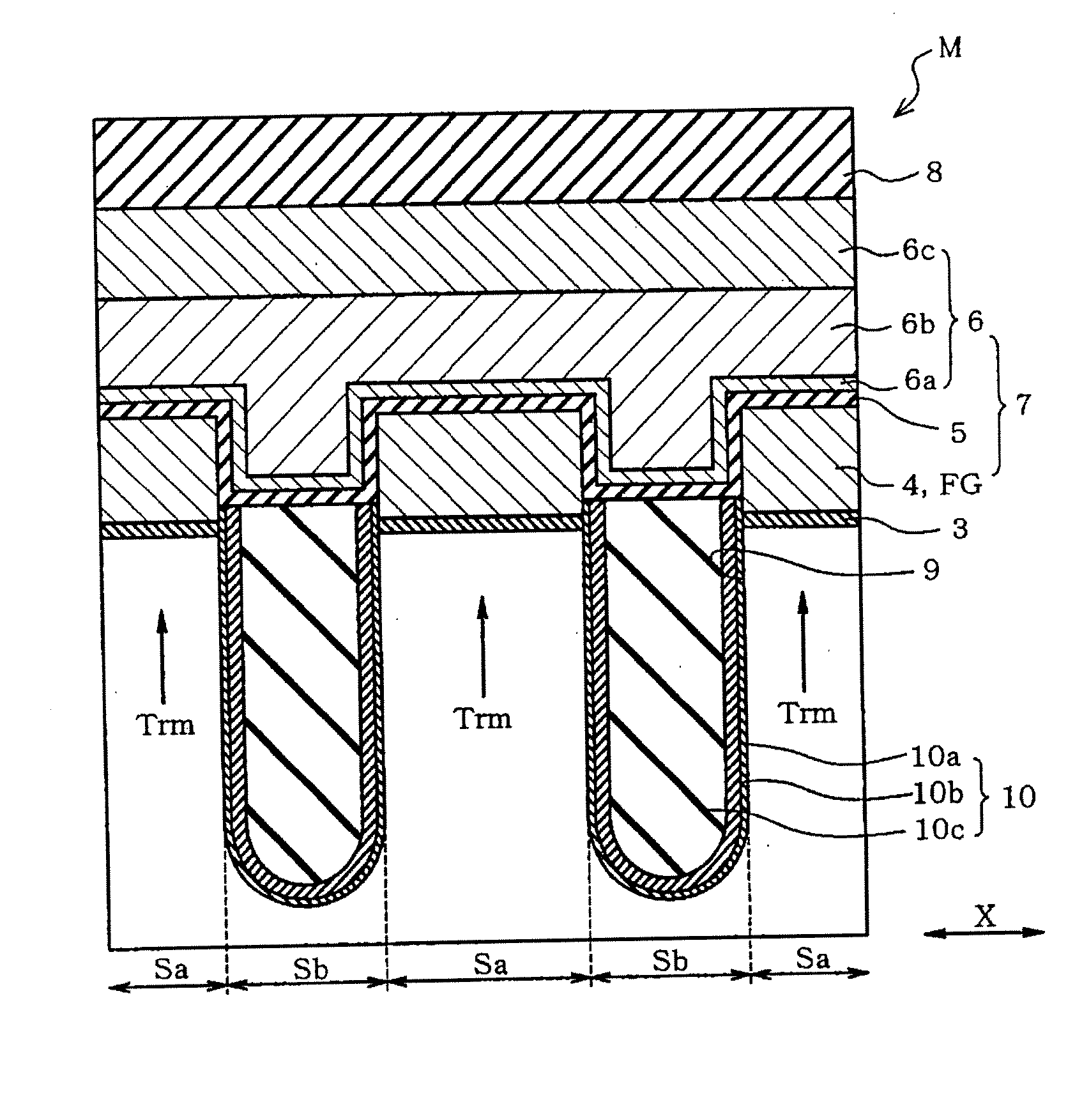
The present invention provides a semiconductor device and a method for fabricating it that can prevent cracking and peeling even when there are different opening widths in the element isolation region. This is achieved by forming a non-coating type silicon oxide film along the inner surface of each element isolation trench with a film thickness equal to or larger than 23 nm, and a coating type silicon oxide film inside the non-coating type silicon oxide film in each element isolation trench. This results in a more robust semiconductor device that can withstand various stresses during the fabrication process.

Problems solved by technology

However, recent miniaturization of elements and reduction in the design rules have increased an aspect ratio in the case where a silicon oxide film is buried in the element isolation trench by the above-described method.
As a result, it has become difficult to fill the element isolation region sufficiently.
When the technique disclosed in JP-A-2003-31650 is applied, the following technical problem arises in a semiconductor device provided with a plurality of element isolation trenches having different opening widths.
The reason for the thermal treatment is that since the coating material has a low density, the etching rate is increased such that the film thickness control becomes difficult during a forming process.
However, since the coating material has a larger film shrinkage factor than the silicon oxide film formed by the CVD method, peeling occurs in the silicon oxide film or crack is produced.
In this case, particularly when an electrically conductive film such as polycrystalline silicon for control gate needs to be deposited on the silicon oxide films, the conductive film enters a peeled portion or crack, whereupon a desired characteristic cannot be obtained.

Method used


Image

  • Semiconductor device and method of fabricating the same
  • Semiconductor device and method of fabricating the same
  • Semiconductor device and method of fabricating the same

Examples


Embodiment Construction

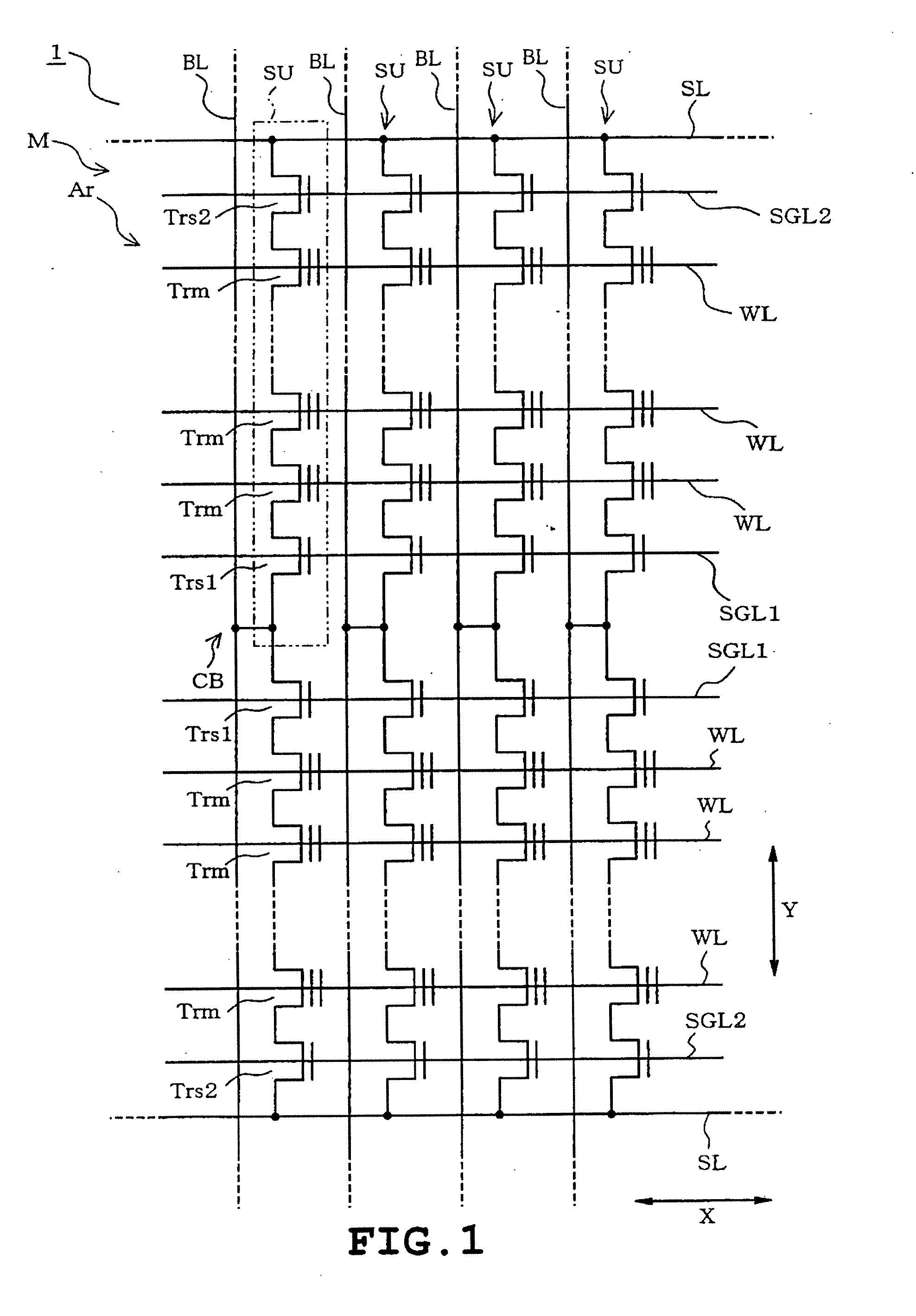
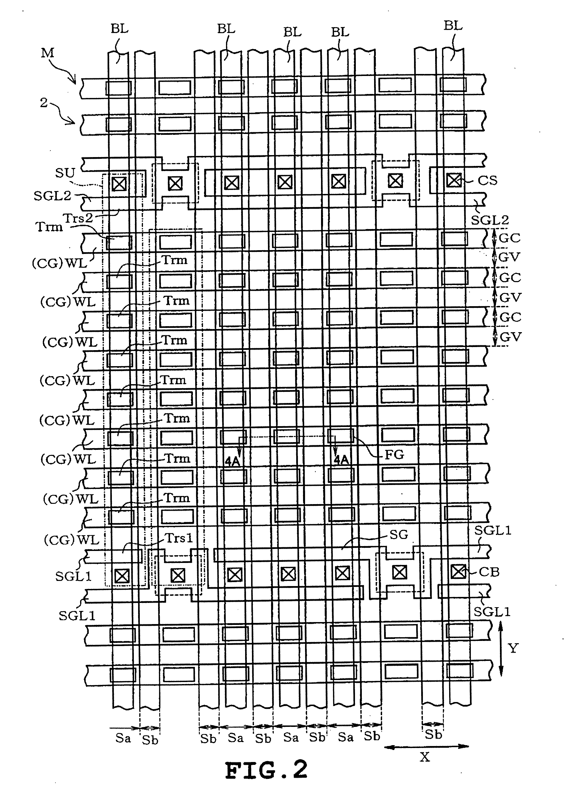
[0023] One embodiment of the present invention will be described with reference to the accompanying drawings. The invention is applied to a NAND flash memory in the embodiment. Identical or similar parts are labeled by the same reference symbols throughout the figures. It is noted that the figures illustrate frame formats of the device and the relationship between a thickness and planar dimension, thickness ratio of each layer and the like differ from those of actually fabricated devices.

[0024]FIG. 1 is a circuit schematic equivalent to a part of memory cell array composed in a memory cell region of the NAND flash memory. FIG. 2 is a plan view showing the structure of a frame format of the memory cell region. FIG. 3 is a plan view showing the structure of a frame format of a peripheral circuit region. FIG. 4A is a longitudinally sectional view showing part of the memory cell region (sectional structure taken along line 4A-4A in FIG. 2). FIG. 4B is a sectional view showing a frame f...


PUM


Abstract

A semiconductor device includes a semiconductor substrate formed with at least two element isolation trenches having a first opening width and a second opening width larger than the first opening width, respectively, a non-coating type silicon oxide film formed along an inner surface of each element isolation trench so as to have a film thickness equal to or larger than 23 nm, and a coating type silicon oxide film formed inside the non-coating type silicon oxide film in each element isolation trench.

Description

CROSS-REFERENCE TO RELATED APPLICATIONS [0001] This application is based on and claims the benefit of priority from the prior Japanese Patent Application No. 2006-270660, filed on Oct. 2, 2006, the entire contents of which are incorporated herein by reference. BACKGROUND OF THE INVENTION [0002] 1. Field of the Invention [0003] The present invention relates to a semiconductor device provided with an element isolation region of the shallow trench isolation (STI) structure and a method of fabricating the semiconductor device. [0004] 2. Description of the Related Art [0005] A shallow trench isolation (STI) method has recently been employed as a method for isolation between elements formed in semiconductor devices. In the STI method, an element isolation trench is formed in an upper surface of a semiconductor substrate, and an insulating film is buried in the element isolation trench so that a predetermined insulating performance is retained. A method for burying a silicon oxide film by ...

Claims


Application Information

Patent Timeline
Patent Type & Authority Applications(United States)
IPC IPC(8): H01L29/00H01L21/762H10B69/00
CPCH01L21/76232H01L27/105H01L27/11531H01L27/11529H01L27/11526H10B41/41H10B41/42H10B41/40H10B41/35
Inventor MATSUNO, KOICHI
Owner KK TOSHIBA
Learn More